How to Layout PCB Power Supply Designs
Think of your PCB layout like a town, figure out power and ground distribution for high-speed, RF, and analog PCB design
Menu
How to Layout Your PCB Power Supply Design
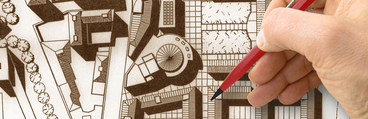
Once you’ve captured a schematic for a high-speed design – or at least some of it – what’s the best way to start placement? I think of a PCB as a bit like a zoned new town like the one I grew up in.
- Separate areas for industrial plants, retail centers, and residential areas
- Good communication within and to the outside world
-
Power and water are supplied separately to each zone. Wastewater is routed carefully before returning to nature. Some water from industrial zones is treated before it joins the rest
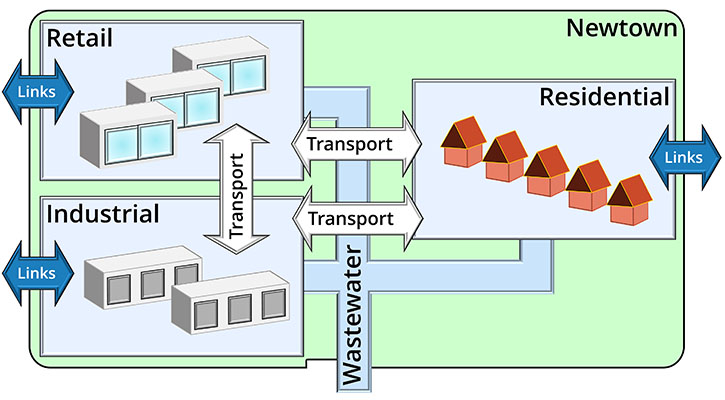
Figure 1: Super-simplified town plan
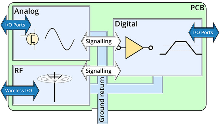
So what are the “zones” for the small Internet of Things (IOT) in PCB? I’ll use it as an example.
- Digital: High-speed, USB, DDR SDRAM, etc. as well as the System-On-Chip that controls it all
- RF: A satellite-tracking antenna
- Analog: Including an Analog-to-Digital (A/D) converter
Starting with the Schematic Design
A little work on the schematic makes things much easier. The first thing I did was to divide the circuit into hierarchy blocks – one for each zone. That’s easy in eCADSTAR and once I did that I could even share them with other engineers. A few components don’t belong to just one zone, so they stayed as they were.
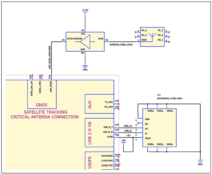
The system-on-chip (SOC) module connects to digital I/O, analog I/O, and an RF antenna. The main module controls analog I/O via a serial peripheral interface (SPI) to an A/D converter and isolation switches, leading to a connector. The A/D converter has both analog and digital I/O, so it is on the boundary between the analog and digital parts of the design.
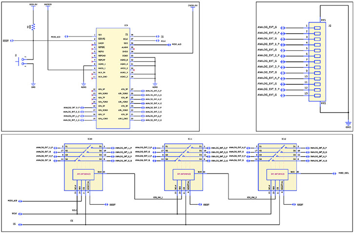
The USB interface is digital and the RF antenna, with its Low Noise Amplifier (LNA) has extremely sensitive and specific routing and grounding requirements.
Initial Placement of Your PCB Power Supply
There are distinct Digital, Analog, and RF parts of the circuit that we can separate in the layout to control the power distribution. The key is to keep ground returns separate until they unite and return to their source. This way, glitches from one circuit don’t affect the others. For example, analog sensors can be very sensitive to ground or power disturbances. In some cases, power goes through “treatments”, just like the town water supply. These are components like ferrite beads, but tellingly they are still called “filters”. They’re there to make sure that even if power is a bit dirty on one side, it’s clean on the other.
In this case, the RF antenna circuit at the bottom left shares its ground return with the digital section, though the application notes warn us to nail ground metal to the main ground plane with plenty of vias.
The analog sensor interface, with its SDI-controlled isolation switches, is at the top.
The division runs through a component just about middle-left. That’s the A/D converter. It has pins connected to both analog and digital power supply buses, so this device straddles the analog and digital areas. This is only a rough placement of an incomplete design, but you can still group components according to ground return and assign them to placement areas in eCADSTAR PCB. That way, none of them will stray off their territory when the design gets more crowded. Provided there are continuous internal ground planes, you can separate areas by the top and bottom PCB surface as well as in the horizontal plane.
Notice anything?
How about that rough division through the A/D converter? Is that in the right place? Could we orient that component better? Best to find out before the design gets denser.
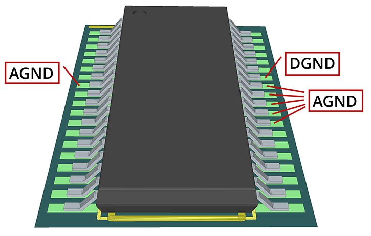
There’s a lot of analog silicon inside this device. The company that makes it even has “Analog” in its name. That’s a big clue. There’s just one digital ground (DGND) but six analog grounds (AGND). The plane split might be better placed along this component’s length instead of its width.
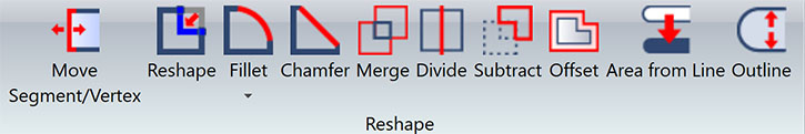
Templates and Shaping for Your PCB Power Supply Design
Once we’ve finalized the design, these rough divisions have to become real copper. That’s where I really like eCADSTAR’s comprehensive template shapes and the intricate adjustments you can make to optimize them. Template shapes adapt automatically to other design changes, and they do it fast, so if you keep components in their areas, the rest takes care of itself.
Checking PCB Power Supply in Detail
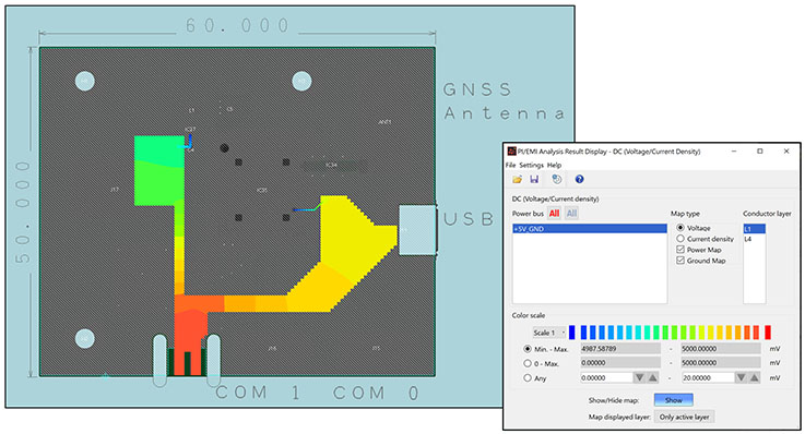
When you think you’ve got it all right, it’s time to make sure. The more you push the design envelope, the more you need this, but it’s still easy to miss important details that could trigger a re–spin. In one design, I’d used the wrong via and only found out when I saw not enough power was getting through to an IC.
It’s well worth checking out the power system buses with eCADSTAR PI/EMI analysis to make sure power distribution isn’t just correct but optimized for maximum resilience. That hardens your design against the unexpected as well as what you’ve thought of. It derives information using the same simulation models as the eCADSTAR signal integrity tools, but you can add to that, for example, by amending via with current thresholds, etc. The more detail you put in, the more you get out. One of the easiest and most useful things to check is DC voltage distribution, but there is far more you can do than that.
Finally Thoughts on Power Supply Designs
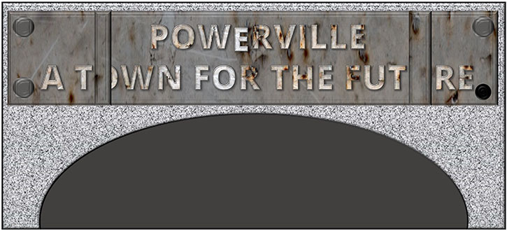
I haven’t shown much detail here. This is just one way to think about it. Power distribution doesn’t stand still any more than, say, memory design. Yesterday’s solutions may not work at all or they may be over-engineered as IC designers get smarter and help us along. It still pays to read the application notes to keep up to date. The town where I grew up was new when we moved there. Above an overgrown pedestrian subway is a rusted sign. It looks a bit like this. The pedestrians go a different way now, and there’s a cycle path.

-
Jane Berrie•Signal Integrity Expert, Zuken Tech Center, Bristol.Jane Berrie has been involved in EDA for PCB signal integrity since the 1980s. Her articles have appeared in many publications worldwide - too many times to mention. Jane is also a past session chair for 3D IC design at the annual Design Automation Conference. Jane’s also an innovator with a unique perspective, who constantly works on new solutions in the fast-evolving world of electronic design. In her spare time, Jane has organized themed charity events - including two in aid of lifeboats and red squirrel survival. Jane is also a regular disco-goer.
A new internet-connected PCB design platform. Get a 30-day eCADSTAR evaluation licence with full features.
REQUEST EVALUATIONReady to brush up on something new? We’ve got more to read right this way.

- Products
March 11, 2024
What's New in eCADSTAR 2024.0
Key highlights of the eCADSTAR 2024.0 update
Read now
The 2024.0 update allows you to meet the increasing demand for compact, high-performing and energy-efficient electronic designs.

- Design Bureau
- VISIT WEBSITE
February 05, 2024
MMD - Modern Micro Devices
Design Bureau
- Blog
February 01, 2024
Power Integrity in PCB Design
Read more.
Read now
Power integrity is a critical stage of successful PCB design. Employing a diverse range of strategies and tools is essential for any designer.

- Blog
November 13, 2023
An Introduction to Time Domain Reflectometers
The TDR has been around for a long time. It’s standard equipment for many engineers, including telecommunications and home broadband installers.
Read now
Time Domain Reflectometer analysis in eCADSTAR’s Signal Integrity Advanced creates results similar to a TDR with simulation. Read More.