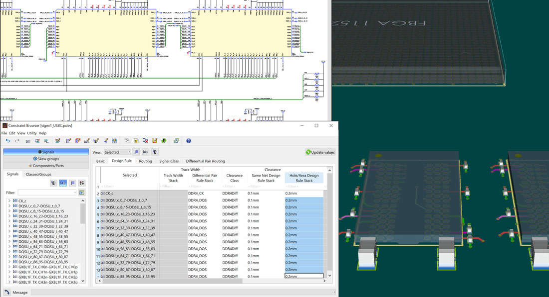
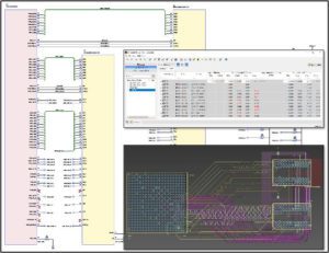
data-migration-1024x450

Constraint-Driven Design

Your constraints defined within your Schematic are carried through to PCB design.
Menu

WHO IS IN CHARGE ?

Meet your electrical performance criteria by setting design constraints. Apply constraints to parts, pins, electrical nets (E-nets), differential pairs and other objects in the Constraint Browser.

CONSTRAINT BROWSER

Setting constraints means you can verify that your design meets standardsinternal or external. And your design follows those constraints as you go, because it costs much less to avoid an issue than to find and fix it later. 
A constraint set early works for you, but consistency is critical. A constraint in library design rules must look the same and work the same as one applied locally, in schematic or PCB. 

Maybe you want to add constraints in the schematic, where you can see what the circuit is doing. Maybe you want to do that during PCB design – selecting items to constrain in physical layout or cross-probing them from schematic. Whatever you prefer, eCADSTAR works with you. Constraint Browser is built into both eCADSTAR Schematic Editor and eCADSTAR PCB Editor

DDR4 strobe routing, Differential pair rule stacks
Necking-down DDR4 strobe routing by switching between differential pair rule stacks as it approaches its controller. Differential pair rule stacks defined in the library can been set as constraints using the unified Constraint Browser in both schematic and physical PCB design.

Design Rule and Constraints

Set or edit constraints in Schematic Editor or PCB Editor. Define technology and design rules in Library Editor. Keep your design settings in sync with your master library or make them local.

Local settings can be useful for prototyping, while synchronized settings are best for production.

Manage constraints in Constraint Browser, in a clearly presented object hierarchy. Look and feel is the same whether you do that in Schematic Editor or PCB Editor.

Forward and back annotation ensure that your constraints are always in syncDefine classes and groups to organize your design and constraints. Create differential pairs and buses. Cross probe selections between the canvas and Constraint Browser in both Schematic Editor and PCB Editor. Highlight objects you constrain by setting colors and taking advantage of visibility options such as shading between differential +/- and E-net pin pairs. 
Route with confidence, assisted by simultaneous display of real-time measurements versus constraints. 

Constraint Browser - differential memory strobes
Constraint Browser showing constraints and results for differential memory strobes

All The Contraints You Need


With eCADSTAR you can:

  • Verify compliance to physical PCB design standards like clearance and creepage rules
Detect inter-layer creepage paths
Detect inter-layer creepage paths between plane areas and copper shapes in 3D
  • Control high-speed signal topology, impedance and skew
construction topology rules and auto-lengthen for skew optimization
Route according to correct-by-construction topology rules and auto-lengthen for skew optimization
  • Verify constraint compliance with built-in, consistent simulation

    Verify signal and power integrity
    Verify signal and power integrity with time and frequency domain simulation

Try eCADSTAR for Free

Start a 30-day free trial with a full-featured evaluation license with no technical limitations. Achieve your PCB design goals today.
Request Evaluation