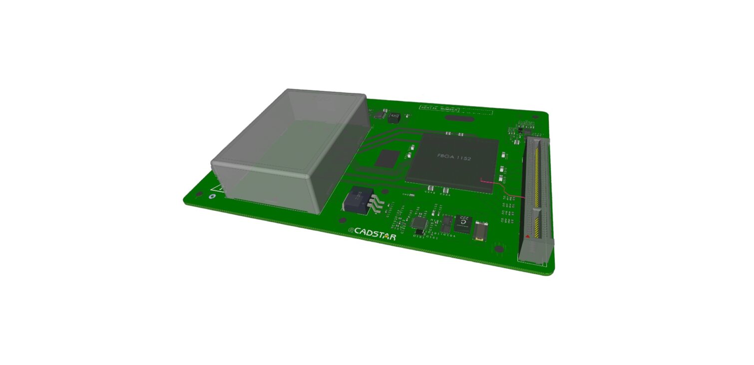
Introduction to PCB Component Design
Printed Circuit Boards (PCBs) serve as the backbone of electronic devices, connecting and powering various components to make them function seamlessly. Effective and efficient selection and placement of PCB components is critical to the overall performance, reliability, and manufacturability of the final product. In this article, we will delve into the world of PCB components, covering essential aspects such as component selection, key information in PCB components, guidelines for effective placement during manufacturing, and the invaluable role of PCB design tools like eCADSTAR.
How to Select the PCB Components You Need
Selecting the right components for your PCB is a critical decision that impacts the overall performance and functionality of your electronic device. Here’s a step-by-step guide to help you make informed choices:
1. Define Your Requirements
Start by clearly defining the functional requirements of your PCB. Consider factors like power consumption, speed, size constraints, and environmental conditions. Understanding your project’s needs is the first step toward selecting the appropriate components.
2. Research Component Specifications
Once you have a clear understanding of your requirements, research the specifications of potential components. Look for datasheets and technical documents provided by component manufacturers. Pay attention to parameters such as voltage ratings, current ratings, package sizes, and temperature ranges to ensure compatibility with your design.
3. Consider Cost and Availability
Cost-effectiveness and component availability are crucial factors, especially for mass production. Compare prices from different suppliers and evaluate the long-term availability of your chosen components to avoid potential supply chain disruptions. Consider alternative suppliers from the outset.
4. Review Quality and Reliability
Choose components from reputable manufacturers known for their quality and reliability. Quality components reduce the risk of malfunction and ensure the longevity of your product. If you are not confident of your entire supply chain, counterfeit components, or cosmetically refurbished components, sold as new, can slip into your products all too easily. If that happens, then even if the product still works, it can fail much earlier than it would with genuine, brand-new components.
5. Ensure Compatibility
Check for compatibility between components in terms of voltage levels, signal levels, and communication protocols. Compatibility issues can lead to circuit failures and operational problems.
6. Allow for Future Upgrades
Anticipate future upgrades or changes in your design and choose components that can accommodate these modifications without requiring a complete redesign. Many recent components, such as DDR5 memory, support pin compatibility, but take care not to make connections to “RFU” (Reserved for Future Use) pins, so you can replace your device with a newer version when those pins come into use.
Important Information on PCB Components
Understanding the key information in PCB components is essential for effective design and troubleshooting. Here are some critical aspects to consider:
1. Component Markings
Component markings include part numbers, values, and manufacturer logos. These markings are essential for identifying and placing components correctly on the PCB.
2. Polarity and Orientation
Certain components, such as diodes and electrolytic capacitors, have polarity and orientation markings. Installing them incorrectly can lead to circuit failure, so pay close attention to these details.
3. Tolerance and Ratings
Components like resistors and capacitors have tolerance values that affect their precision. Ratings, such as voltage and current ratings, should be well within the specified limits to prevent overloading and component failure.
4. Temperature Coefficients
Temperature coefficients indicate how a component’s performance changes with temperature variations. This is crucial for stability in different operating conditions.
PCB Component Placement Guidelines for Manufacturing
Effective PCB component placement is essential for ensuring smooth manufacturing processes and optimal circuit performance. Follow these guidelines:
1. Group Components by Function
Organize components into functional groups based on their roles in the circuit. This helps minimize signal interference and simplifies troubleshooting.
2. Keep Critical Components Accessible
Place critical components, such as microcontrollers and voltage regulators, in easily accessible locations. This simplifies testing, debugging, and potential replacements.
3. Minimize Trace Lengths
Where possible, shorten signal trace lengths to reduce signal propagation delays and electromagnetic interference (EMI). This is especially important for high-speed digital circuits. Optimize chipset placement as much as possible.
4. Maintain Proper Spacing
Ensure adequate spacing between components to prevent overheating and ensure good airflow. Components that generate heat should have sufficient ventilation and the ability to dissipate heat. Datasheets and application notes sometimes suggest how to connect conductor areas on the base of the component body, which can assist thermal conduction and dissipation.
5. Follow Design for Manufacturing (DFM) Guidelines
Adhere to DFM guidelines provided by your manufacturer. This includes respecting minimum clearances, component pad sizes, and other manufacturing-specific requirements.
How PCB Design Tools like eCADSTAR Can Help Create the Best Component Placement
Modern PCB design tools like eCADSTAR offer powerful features to streamline the component placement process and enhance overall design efficiency:
1. Interactive Placement
These tools provide interactive placement features that allow designers to easily move and rearrange components on the PCB layout, ensuring optimal positioning and efficient use of board space.
2. Real-Time Design Rule Checking
eCADSTAR and similar tools incorporate real-time design rule checking, helping designers identify placement issues such as clearance violations, trace routing problems, and component collisions as they work, including in 3D.
3. 3D Visualisation & Checks
They offer 3D visualization capabilities, allowing designers to see how components will physically fit on the PCB and how they interact with other elements, ensuring proper clearances and minimal interference.
4. Collaboration and Simulation
These tools enable collaboration among design teams and often provide simulation features to assess signal integrity, thermal performance, and other critical aspects of component placement.
5. Re-use Blocks of Test and Proven Designs
In eCADSTAR, you can use board blocks to maximise design re-use, with optimum design integrity and great time management. Your team can work on these blocks independently and merge or re-merge them together with their designs in an intelligent and efficient PCB design process.
In conclusion, mastering PCB component design is vital for the success of any electronics project. Careful selection, understanding key component information, following placement guidelines, and leveraging advanced PCB design tools can help you create PCBs that not only meet your project’s requirements but also ensure reliability and manufacturability. By adhering to these principles and harnessing the capabilities of tools like eCADSTAR, you can design PCBs that excel in performance and efficiency.

-
Jane Berrie•Signal Integrity Expert, Zuken Tech Center, BristolJane Berrie has been involved in EDA for PCB signal integrity since the 1980s. Her articles have appeared in many publications worldwide - too many times to mention. Jane is also a past session chair for 3D IC design at the annual Design Automation Conference. Jane’s also an innovator with a unique perspective, who constantly works on new solutions in the fast-evolving world of electronic design. In her spare time, Jane has organized themed charity events - including two in aid of lifeboats and red squirrel survival. Jane is also a regular disco-goer.


