Check 3D PCB Creepage in eCADSTAR

What is PCB creepage and why worry about it?
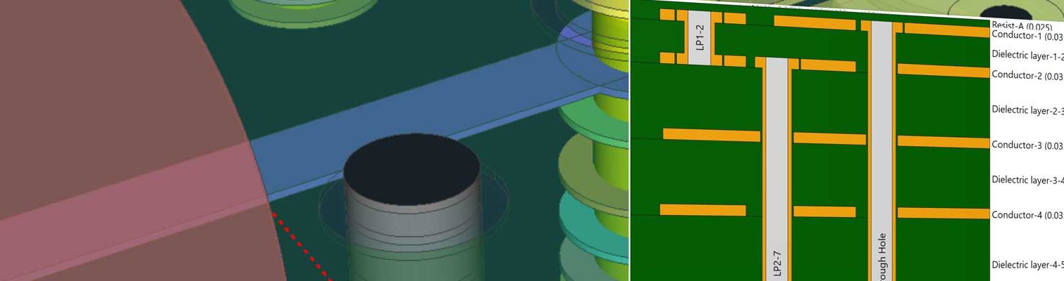
2D clearance is always less than or equal to 3D clearance. Working to 3D creepage rules means you can design more densely because clearance is measured by its true path. As well as lengthening a creepage path, a slot or hole can create an additional one in the third dimension as it is does here.
Creepage vs clearance
Clearance is the distance between objects from point to point, in 2D or 3D. The difference with a creepage check is that it considers the 3D path across the PCB. You can think of this as the terrain. Imagine a traveller walking between two villages. If they measure the distance on their map in a straight line with a ruler, that’s the clearance distance. But if there is a valley or mountain between the two villages, the distance the traveller walks will be longer than the clearance. That distance is like the creepage distance. Creepage distance is important, because sometimes you can increase the travel distance between two objects without having to move those objects further apart.
Creepage is the leakage of electrical current across the surface of an insulator.
There are two main things that make a creepage issue more likely:
- High voltage difference between two objects.
- Pollution/contaminants.
The creepage check has to know the voltage differences between objects on the PCB. For DC, you can set the voltage on each object and the voltage difference is based on the difference between those two values.
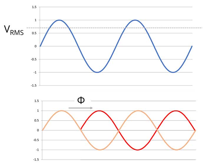
With AC signals, you have to consider relative phase.
Contaminants and pollution affect current leakage across surfaces and so expected environment is an important consideration. A damp surface is more prone to leakage than a dry one. Maybe the PCB is close to machinery and prone to vapor or oil misting.
Creepage is an important consideration in high-voltage PCB design guidelines—often applied to much higher voltage differences than the example illustrated here. Hundreds or thousands of volts. In such PCBs, although many more subtle PCB features come into play, a solid 3D creepage check is a good baseline.
Setting up useful and meaningful creepage checks
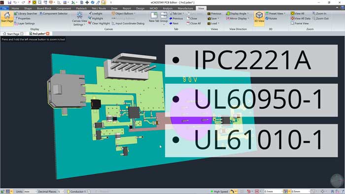
Clearance and creepage standards like IPC2221A, UL609050-1, UL-61010-1 and the more recent IEC 62368-1 (superseding 60950-1 and 60065), are graded according to defined pollution levels and cover many topics related to PCB design safety.
You can apply standards by defining them as Voltage Difference Clearance Tables.
You can enter rules that represent published standards as Voltage Difference Clearance Tables as well as defining your own for in-company standards.
You can include layer-dependent rules and AC phase groups. You can share voltage difference clearance rules with other engineers, independent of other design rules.
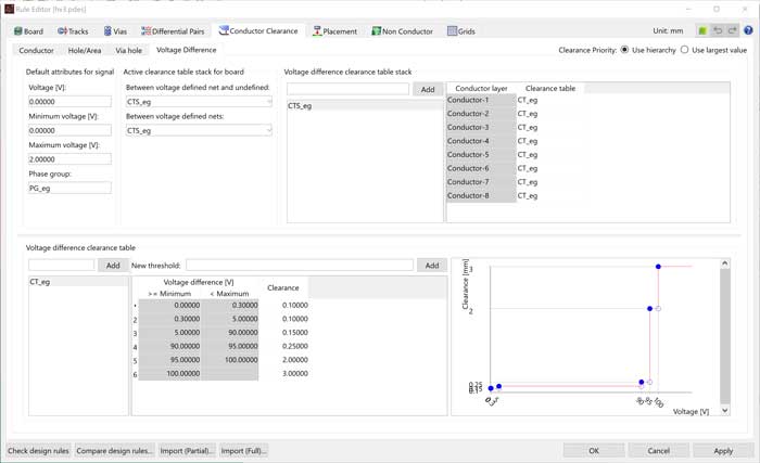
Voltage Difference Clearance Table Stacks can include layer-dependent rules.
You can set creepage rules in your master library or local design rules. You can apply them in a hierarchy. Constraint levels include whole board, differential pair class, differential pair, E-net class, E-net, net class, (logical) net and rule area.
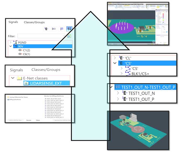
You can apply creepage rules where you need them and not elsewhere, with the choice of applying the strictest rule or the one in the highest-priority position in the hierarchy.
Use results to dynamically optimize electrical safety and layout density
Once you have set of creepage rules, you can check objects for creepage. Checking for creepage in 3D gives you two major advantages:
- You can check effectiveness of 3D elements like slots to break or lengthen creepage paths, meaning you can pack components more densely.
- You can check for unexpected Z-axis creepage paths through the PCB created by holes and slots.
When you check creepage, you can choose a Modelling Accuracy level. Higher modelling accuracy provides more detailed analysis and takes longer. Creepage checks are made from selected objects. A typical selection would be a high-voltage bias or power signal. Search Distance is the maximum distance from those selected objects to be considered by the creepage check. The check reports creepage distances that are OK according to the rules you set as well as those that are in error. A larger Search Distance increases the time taken to generate the report. You might set Search Distance to twice or three times the minimum allowed clearance.
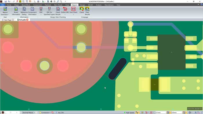
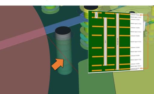
The circular shape is a 90V avalanche diode bias signal for a LIDAR system. This has to be kept clear of the nearby -5V supply, but space is tight. The length of the 3D creepage path has been increased by adding a slot, instead of increasing clearance in the horizontal plane. On the first attempt, the slot is not quite in the right position, so the creepage check fails. A red line is displayed on the PCB Editor canvas, showing the creepage path.
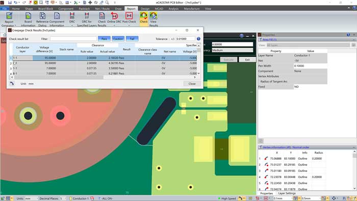
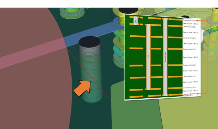
After moving the slot, the creepage path is long enough to pass the check, but a white line still displays the path to allow further optimization.
More detail in video
Related Content
- Products
Zusammenfassung der Ausgabe 2021

- Products

- Products