In the current era, printed circuit boards (PCBs) are subjected to progressively rigorous design stipulations. This phenomenon can be attributed to two key factors: the persistent drive to transmit increasingly elevated data rates and the concomitant necessity to guarantee robust signal integrity.
In the low frequency range, simplifications are possible by neglecting the electrical parameters, but with increasing frequency ranges, physical effects manifest themselves that require consideration of all different aspects, the material properties, the geometry and the arrangement on tracks in relation to each other. Dispersive material properties, the skin effect, the loss dielectrics, reflections and radiation effects should be mentioned here. Problems caused by lossy dielectrics and stubs occur in particular at higher frequencies. When designing PCBs with high-speed transceivers, special attention must be paid to sharp close to rectangular pulses (very fast digital signals), as these have a broad spectrum with many frequencies to compose them. The steepness of the edge defines the respective edge frequency.
This means, that each frequency component in a pulse may “see” a different transmission path. As analyzing each frequency component in the spectrum of the pulse involves a great effort, it is recommended that you limit yourself to just looking at the overall spectrum. It is recommended to analyze the pulses in the time domain. The eCADSTAR software offers the user the option of simulating high-speed SerDes channels using IBIS-AMI models and thus making a high-quality assessment about the quality of the data connection.
Design Challenges in High-Speed Data Transmission
As part of the development of an EMUS (electromagnetic ultrasound) multi-channel system a backplane was developed at the Fraunhofer Institute for Non-Destructive Testing via which up to four EMUS modules can exchange data with each other and with a central processing module. Several billion bits per second will be transmitted on the backplane. The backplane also offers the option of distributing a common time base and synchronized trigger signals to all the connected modules, which is the basic prerequisite for the use of a multi-channel network system, for example as a phased array. As main control unit of each of these EMUS boards acts an FPGA (Field Programmable Gate Array) from the Zynq-7000 series from Xilinx. The FPGA is equipped with several GTX transceivers, which enable a maximum transfer rate of 12.5 Gbps. A schematic structure is shown in Figure 1.
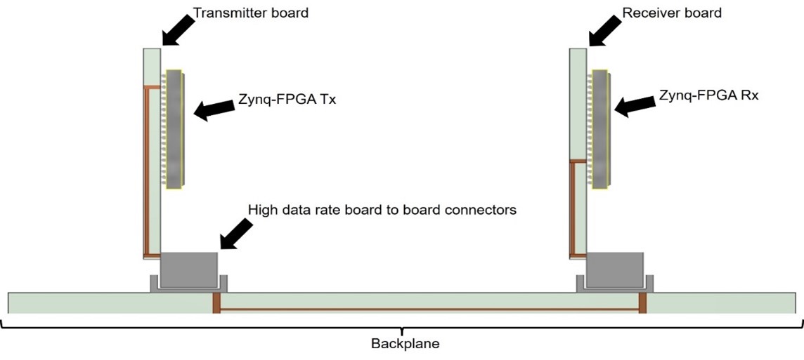
Figure 1 Backplane with transmitter and receiver board
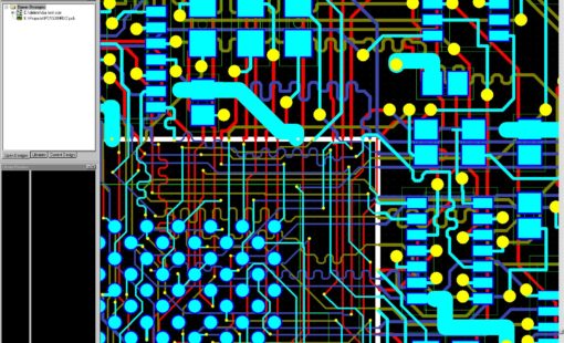
As part of this development, a layout was created that had to fulfil the complex requirements with respect to signal integrity. The target defined here was a successful data transmission rate of 7.5 Gbps, which had to be achieved as part of my bachelor’s thesis. Another aim of this thesis was to carry out a study where the properties of conventional materials, RF materials and stubs have been analyzed in relation to the eye opening of the channel.
Physical basics
Lossy dielectrics
The term dissipation factor is often used to describe the loss characteristics of a dielectric.
In physical terms, the losses in the dielectric are caused by polarisation. Dielectric materials have a conductivity σ ≠ 0, which is referred to as ohmic loss. When an AC voltage flows across a conductor path, an electric field builds up between the forward and return conductors (in the case of PCB structures, corresponding to the microstrip conductors and the reference layer). This leads to an alignment (rotation) of the dipoles in the intervening dielectric.
Dispersive material
In the presence of a dispersive material, the and change with increasing frequency (f = 2π/ω). The propagation speed of a signal in a medium can be calculated using the following formula:
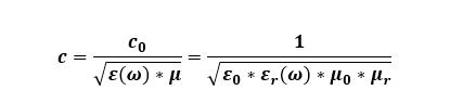
Here, C0 is the propagation speed of the signal in a vacuum or the speed of light. This implies that a signal that perceives a different εr will always have a different propagation speed. In the case of a rectangular pulse composed of several by of multiple different frequencies, it can be deduced that the spectral components of a rectangular pulse will always drift further apart.
Stubs and VIAs
On a printed circuit board, conductive paths can cut off each other so that signals cannot pass on. The signal layers on a circuit board are be changed by means of a through-hole connection. This type of through-hole plating structure is known as via (vertical interconnect access)
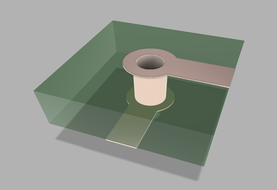
Figure 2 Vias
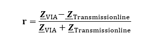
Vias have a complex structure that makes it difficult to adapt them to a desired line impedance. The geometric properties of a via are responsible for this. The reflection between a via and transmission line can be derived according to the following equation:
The reflection of the transmitted signal due to the impedance differences between the line and via can cause another problem if not handled correctly in a layout. If a via is not connected to a line at its end, this short segment will act like an LC resonant circuit. Consequently, this stub shows resonances in the frequency range. In the situation of a signal with a frequency close to or around such a resonance of the stub, the signal will be strongly attenuated due to the maximum energy requirement of the stub at this frequency. Alternatively, the stub stores all the incoming energy and does not allow any further propagation. In both cases, the via stub can be described as a bottleneck for a signal at this frequency, which may lead to maximum attenuation at this particular frequency.
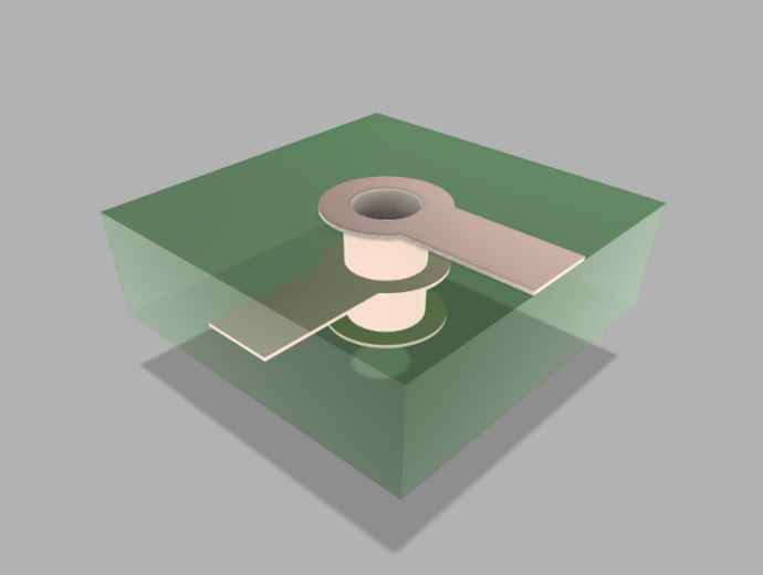
Figure 3 Via Stub
Eye diagrams
The signal integrity of rectangular signals is often checked in the time domain, as analysing the individual frequency components in the frequency domain involves huge efforts and is only of limited significance with regard to the quality of the signal transmission. To avoid having to analyze an entire bit-stream in the time domain, the rising and falling edges of all the bits under consideration are superimposed and presented for visual inspection or automatic measurements. The resulting diagram is referred to as an eye diagram. The conditions that must be met by an eye diagram in order to guarantee proper data transmission are usually specified in the data sheets of the respective transceivers.
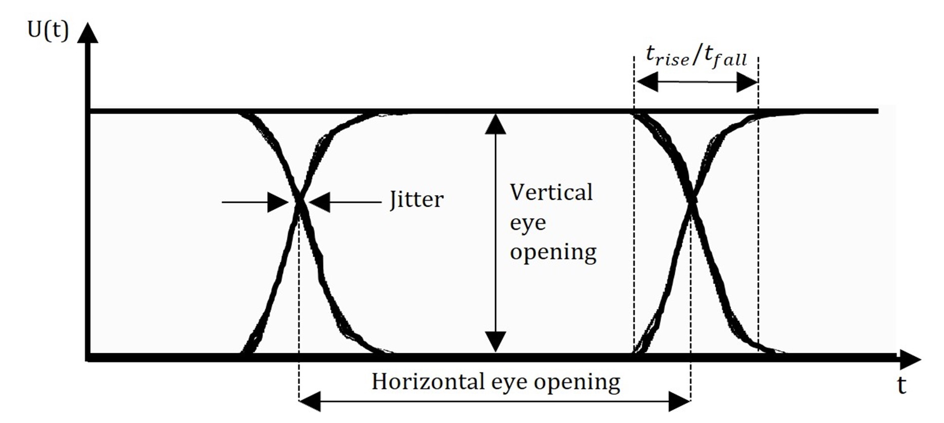
Figure 4 Eye diagrams
So called “Eye masks” whose definition is based on the unit interval are used to visually check the eye diagram for meeting the requirements. This reduces the amount of constraint data, as an eye diagram does not have to be stored in the data sheet for each data-rate to be checked. The parameters are calculated using the following equation:

Simulation of the GTX SerDes Backplane Channels:
The structure to be analysed is a SerDes channel where the connections between transceiver and receiver are implemented using differential impedance-matched transmission lines with an impedance of Zdiff = 100 Ohm.
In order to display the eye diagrams of the transmission path at a data rate of 7.5 Gbps, it is necessary to define the corresponding parameters. The physical structure, composed of frequency-dependent, lossy dielectrics, vias, stubs, connectors and pads, is automatically converted into an equivalent circuit diagram. The eCADSTAR software supports the creation of the equivalent circuit diagram from the layout of the channel which should be analysed. The connectors, which serve as the link between the backplane and the transmitter or receiver card, can either be assumed to be ideal or described by an S-parameter file which will be assigned to them. The schematic structure is shown in the following figure.
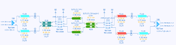
Figure 5 Schematic structure of the SerDes channel
In order to be able to simulate the structure to gather eye diagrams, the information of the driver and receiver must first be assigned to the simulation structure. This is done by assigning IBIS-AMI models which have been derived from the IC vendor (here Xilinx) and imported into the software. IBIS stands for « Input/Output Buffer Information Specification ». An IBIS model contains on black-box level information about the current/voltage ratio of the I/O buffer and the all relevant RLC parameters of the individual pins of the receiver and transmitter. AMI stands for “Algorithmic Modelling Interface”. Such AMI blocks contain information that models the internal functionality in the transmitter and receiver.
SerDes-Simulation of the Eye Diagrams
The optimized workflow in eCADSTAR enables a simulation to be carried out very efficiently. It is recommended by Xilinx that the first 100,000 bits are skipped from the SerDes simulation. A total of 200,000 bits have been simulated of which the first 100,000 bits were excluded from the analysis in accordance with the manufacturer’s specifications. The eye diagram generated by the eCADSTAR software is shown in the figure below.
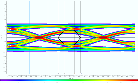
Figure 6 Eye diagram at 7.5Gbps
For the use of eye masks, eCADSTAR offers the option of creating these and using them to check signal integrity compliance. The eye mask shows that a successful data transmission is likely not possible based on the observation from signal-pin to signal-pin, taking into account the given layout pattern. The software also allows to measure of the percentage of the eye opening, which is 70.9% in the diagram above.
In order to determine whether the PCB material currently used for impedance matching has too high losses or the permittivity varies too much over frequency, a simulation has been carried out with a higher quality material which has a significantly lower tan φ. For this purpose, the parameters have been applied to the Rogers Corp. material, type RO3003, with has a dielectric constant of εr = 3 and a tan φ = 0.01. Previously, a material with a dielectric constant of εr = 3.8 and a tan φ = 0.04 has been used. Adjusting these parameters in the simulation will results in an eye diagram with an eye opening of 77.8 %, hence a better behavior with respect to signal integrity.
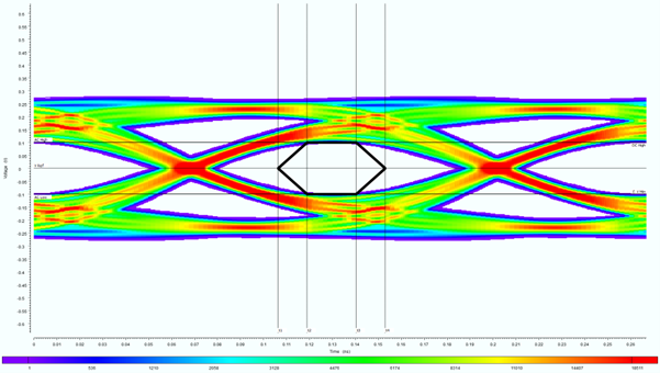
Figure 7 Eye diagram at 7.5 Gbps with RO3003
Such special materials are often used for high-frequency applications, but they are significantly more expensive than conventional FR4 materials. Although an improvement in transmission quality has been achieved with the new material, another aspect has been investigated also. Initially, a number of vias and stubs has been present in the transmission channel. The simulation has therefore been adapted accordingly in order to remove the vias from the channel path. The conventional standard material has been used again. The simulation without vias/stubs leads to an improvement in the eye opening of 13.3% compared to the previous simulation in Figure 6 (total opening of about 84%)
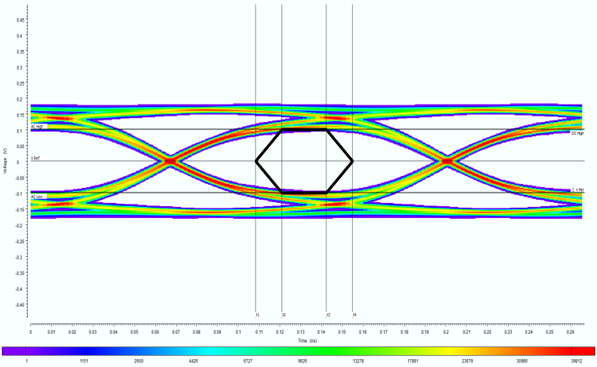
Figure 8 Eye diagram at receiver at 7.5 Gbps without vias and eye opening 84.2%
From a layout perspective, it is currently not possible to implement all these changes. However, it should be noted that so far only the eye diagrams from the driver pad to the receiver pad have been investigated. By using IBIS-AMI models, eCADSTAR offers the possibility to view the eye diagrams at the receiver as well. Many FPGAs know chip-internal filters or equalizers which are implemented in the receiver architecture of the high-speed transceivers. These are mapped by the AMI part of the model, whereby the equalizer settings can be modified depending on the transmission protocol so that the eye diagram will be opened further or the eye diagram can be displayed on a probing position in the receiver after the chip-internal equalization stage.
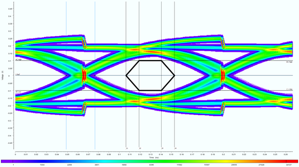
Figure 9 Eye diagram after equalisation at 7.5 Gbps with eye opening 86.6%
Figure 9 shows that the internal equalizers in the receiver can reconstruct the eye diagram to such an extent that, compared to Figure 6, data transmission at 7.5 Gbps is possible without adapting the layout or materials.
Conclusion:
The development of high-speed SerDes channels for the transmission of large amounts of data defines high complex requirements on the signal integrity of such printed circuit boards because of both, the increasing demand for higher data rates and the need to take physical effects precisely into account. In low frequency range, simplifications can be used by neglecting the electrical transmission line parameters and parasitics. In higher frequencies, however, dedicated physical effects occur due to dispersion, skin effect, lossy dielectrics, reflections and radiation, which require detailed consideration.
The simulation of high-speed SerDes channels using IBIS-AMI models in eCADSTAR enables an accurate assessment of signal quality and aperture. By examining different materials, such as RO3003 compared to conventional FR4 materials, and customizing the channel structure by removing vias and stubs, significant improvements in transmission quality can be achieved. The analysis of the eye diagrams on the transmitter and receiver side enables a comprehensive evaluation and optimization of the channel integrity.
Finally, it is clear that successful data transmission at high data rates depends not only on the selection of high-quality materials and careful channel design, but also on the implementation of suitable signal processing techniques in the receiver. By taking all these aspects into account, the quality of the data link can be optimized and reliable transmission of large amounts of data can be guaranteed.