
CADSTAR Rules-by-Area - Datasheet

TOP FEATURES AND BENEFITS
- benefits you when you are forced to compromise your design rules when using BGAs
- helps you when yield is a problem in the design of fine-pitch devices
- incorporate overlapping areas that can be any shape into your designs
- lets you copy areas, while also obtaining and copying the associated technology restriction rules
Introduction
Today’s products require more functionality in ever reducing spaces, resulting in the need to achieve increasing density of the placement of components on a PCB. Additionally many circuit boards are being designed with a mix of digital and analogue circuits, each requiring the use of different rules and constraints when routing.
With the reduction in size, the pin pitch of the component compounds the complexity and difficulty of the design, resulting in a design where manual alterations must be done, for example, to connect component pads to routes.
 There are different methods to solving these problems, ranging from using higher layer-count boards and thinner track widths and spacing, to using the option of blind- and buried-via technology depending on the design requirements. Increasingly, the designer is having to use a mixture of these solutions on the same board. This causes the frustrating problem that the design rules that are acceptable for a major part of the board design, cannot be used in other areas of the design.
Rules-by-Area
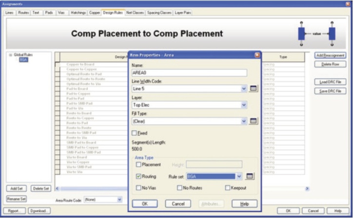
The Rules-by-Area package is a powerful extension to the CADSTAR P.R.Editor XR 2000 tool-set that enhances Zuken’s routing technology by allowing the association of different design rules to different areas of the design.
With Rules-by-Area, tracks can be reduced in width according to the rules defined by the area they are routed through. It is now possible to execute the routing manually or automatically. Other rules that can be defined for specific areas include via sizes and also the use of blind or buried via technology.
Spacing rules for any area may be redefined which is especially useful around small complex dense components such as BGAs, Wire Bonded CSPs and SMDs allowing for 100% error free routing.
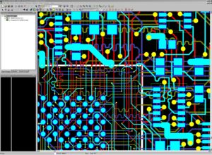
High speed routing will also obey the rules defined by the area. There is no limit to the number of areas that may be defined, and these areas may be of any shape and on any layer desired.
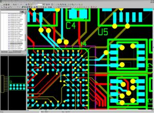
Design Rule Checks by Area
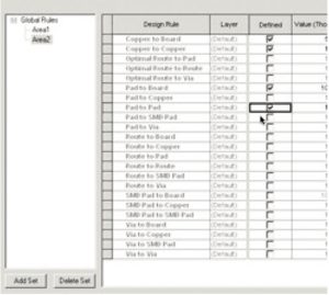 Required routing rules for each area are added in CADSTAR. The designer can take advantage of the online design rules checking feature in P.R.Editor, while routing in areas with the alternative rules set. This will highlight any error condition as defined by the rules for the current area with the further advantage that all areas may be routed error free without the need to change the routing rules that are obeyed.
Knowing that all the design rules will be obeyed, the designer can auto-route the entire PCB, or route manually with the tool highlighting any non-compliance to the pre-set constraints.
Fully definable rule sets per area
For each area that is placed on the design you can set different track spacing, net routing widths and a via sizes. This gives outstanding routing flexibility when specifying and using micro-vias, fine-line and very small tracks, vias and pad spacing.
CADSTAR Rules-by-Area Solution Features
- Definable routing widths
- Definable via technologies per area
- Alternative spacing rules per area
- Online design rules checking
- Can be defined on any layer
More
 CADSTAR is a fully featured PCB Design System renown for its excellent price-performance ratio. From simple single-sided through-hole designs to multi-layer, surface mount, highspeed digital and analogue designs, CADSTAR is capable of designing today’s most demanding Printed Circuit Boards. From schematics, board- and FPGA level system design, PCB layout, high-speed and signal integrity, analysis, 3D, creation of manufacturing output, to complete data management capabilities and extensive internet-accessible libraries containing over 200,000 components, CADSTAR provides you with all technologies necessary for a complete electronic development process in one environment.
 CADSTAR Rules-By-Area – Datasheet
Ready to brush up on something new? We’ve got more to read right this way.

- Solutions
Mise à niveau aujourd'hui
- Products
Grâce à une multitude de fonctions standard et de modules complémentaires, eCADSTAR vous permet d'adapter votre offre de conception pour répondre à vos besoins en matière de conception de PCB