
5 Common Mistakes PCB Designers Should Avoid
Printed Circuit Board (PCB) designers play a crucial role in the electronics industry, bridging the gap between conceptual designs and functional devices. However, even the most experienced designers can make mistakes that can have a significant impact on the final product’s performance and reliability. In this article, we will explore five common mistakes that PCB designers often make and provide insights on how to avoid them. By being aware of these pitfalls and implementing preventive measures, designers can enhance their design processes and produce high-quality PCBs.
Insufficient Component Placement Considerations
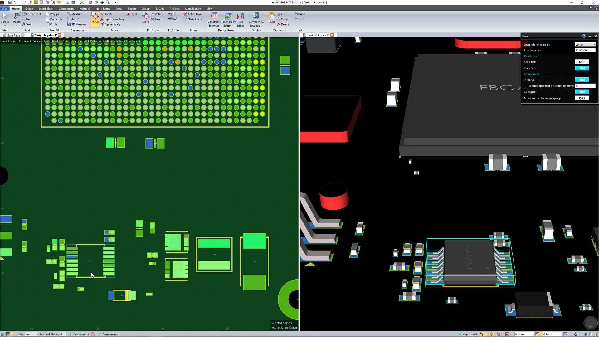
One of the most critical aspects of PCB design is component placement. Often, designers overlook the significance of proper component placement, leading to a range of issues. Insufficient consideration of component placement can result in signal integrity problems, increased noise, thermal issues, and even difficulties in the manufacturing process.
To overcome this mistake, designers should consult with manufacturers early in the design phase. They should consider factors such as layerstack, panelization, component footprints, solder mask clearance, minimum trace widths, and drill holes. Some components, like Buck Regulators (used in DC-to-DC supply voltage conversion) are more placement-critical than they appear, because internally, they use high-frequencies, even when, as in this case, they are controlling DC. Suppliers such as Analog Devices sometimes supply recommended layouts for their devices and attached components, to give you a head start. Typically, this is supplied as Gerber data, which can be imported and mapped to other PCB layer stacks in an EDA application such as eCADSTAR PCB Editor.
By following best practices and consulting design guidelines, designers can optimize component placement and improve overall PCB performance.
Inadequate Power and Ground Plane Design
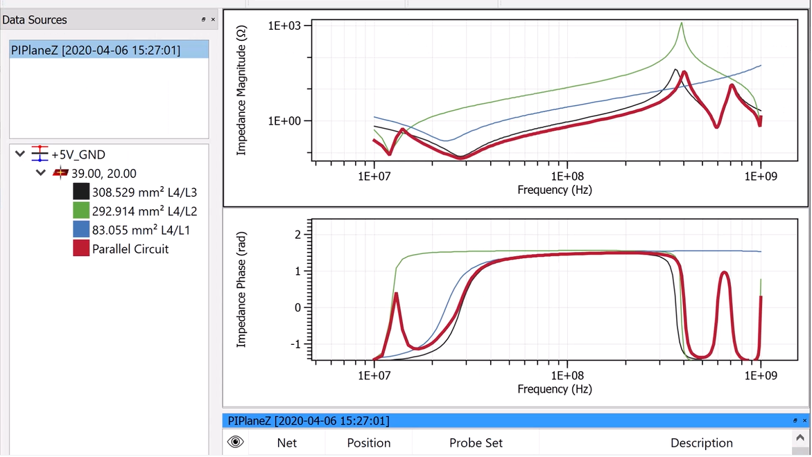
Power and ground planes serve as the backbone of any PCB design, providing stable power distribution and reducing noise. However, designers often make the mistake of neglecting their importance or improperly implementing them. This oversight can result in power delivery issues, EMI problems, and decreased signal integrity.
To avoid this mistake, designers should allocate sufficient space for power and ground planes. They should follow the recommended layer stack-up and ensure appropriate decoupling capacitor placement near critical components. By adhering to proper power and ground plane design principles, designers can minimize noise and enhance signal integrity.
In controlled-impedance designs, it is essential to route signals adjacent to their own ground and power planes. Without that, noise will escalate, and impedance control will not work properly. In some designs, for example, there are both analog and digital grounds. Even if these grounds represent the same root signal, their plane areas must often be kept apart until they reach a point near their source – typically at a connector,
Neglecting Design for Manufacturability
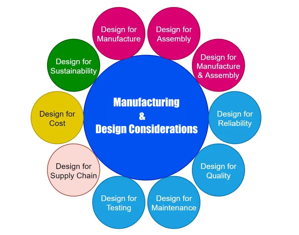
Designing a PCB without considering the manufacturing process can lead to complications during fabrication and assembly. Neglecting Design for Manufacturability (DFM) guidelines can result in increased production costs, longer lead times, and potential reliability issues.
To overcome this mistake, designers should consult with manufacturers early in the design phase. They should consider factors such as panelization, component footprints, solder mask clearance, and minimum trace widths. By involving manufacturers from the beginning and incorporating DFM principles, designers can ensure a smoother production process and avoid unnecessary setbacks.
Additionally, each manufacturer has preferred “default” layerstacks, and the minimum hole size can drastically impact the cost of a PCB. For example, 0.2mm is the current industry standard, so should you want a 0.1mm hole the price would increase. The smaller the via the less space you need but ultimately you would want to produce the board with as little scrap as possible.
Ignoring Thermal Management
PCB components generate heat during operation, and inadequate thermal management can lead to premature component failure or degraded performance. Unfortunately, many designers overlook thermal considerations, assuming the heat dissipation will occur naturally.
To avoid this mistake, designers should evaluate the thermal characteristics of components and incorporate proper heat sinks, thermal vias, and copper pours. They should ensure sufficient spacing and airflow within the enclosure. Utilizing thermal simulation tools can also help identify potential hotspots and optimize thermal management strategies. By addressing thermal concerns proactively, designers can enhance the reliability and longevity of their PCB designs.
Overlooking EMI/EMC Compliance
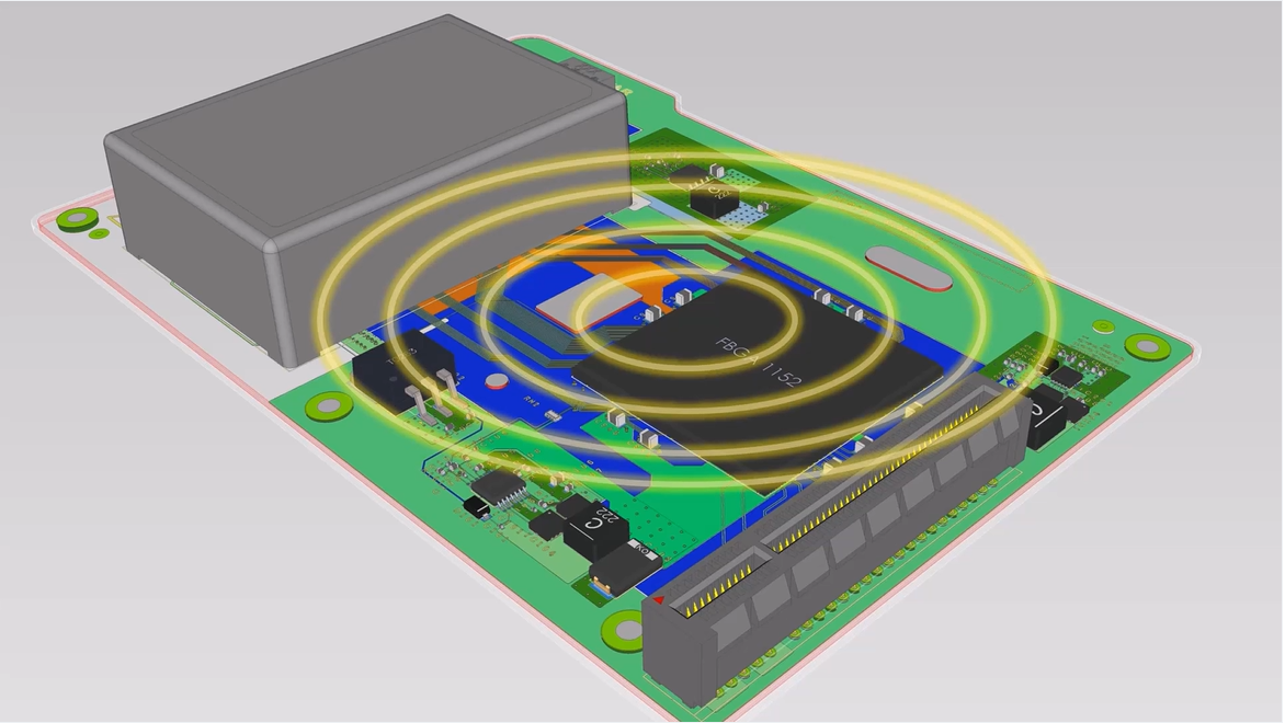
Electromagnetic Interference (EMI) and Electromagnetic Compatibility (EMC) issues can lead to functional disturbances and failures in surrounding electronic devices. Unfortunately, many designers fail to consider EMI/EMC compliance until the later stages of the design cycle, leading to costly and time-consuming revisions.
To avoid this mistake, designers should incorporate EMI/EMC considerations from the outset. They should carefully route high-speed traces, employ proper shielding techniques, and utilize EMI filters, such as ferrite beads to block conducted external spikes, and common-mode filters, to stop non-differential signals being transmitted via differential pair routing, as necessary. By following design guidelines and performing pre-compliance testing, designers can minimize EMI/EMC issues and ensure their PCB designs meet industry standards.

-
Jane Berrie•Signal Integrity Expert, Zuken Tech Center, BristolJane Berrie has been involved in EDA for PCB signal integrity since the 1980s. Her articles have appeared in many publications worldwide - too many times to mention. Jane is also a past session chair for 3D IC design at the annual Design Automation Conference. Jane’s also an innovator with a unique perspective, who constantly works on new solutions in the fast-evolving world of electronic design. In her spare time, Jane has organized themed charity events - including two in aid of lifeboats and red squirrel survival. Jane is also a regular disco-goer.

- Blog

- Blog

- Blog
Discover how Quadra Solutions won the prestigious award and what it takes it win!
- Blog
Read more!