
Your eCADSTAR Library: Enter Less, Re-Use More
Hierarchy Yields Efficiency
The library is structured so you enter the minimum data and re-use it to the maximum. One example is the hierarchy of layers and layer stacks. You start with a minimal set of footprint layers. PCB Technologies, Padstacks, and Footprints map to these generic layers, but still in a way that means you can use them with the widest-possible variety of PCBs. Design Rules take the data to the final level you use in your PCB design, with a fully defined and detailed layer stack.
You can add as much detail as you will possibly need, when and where you need it, but efficiency and re-usability are key.
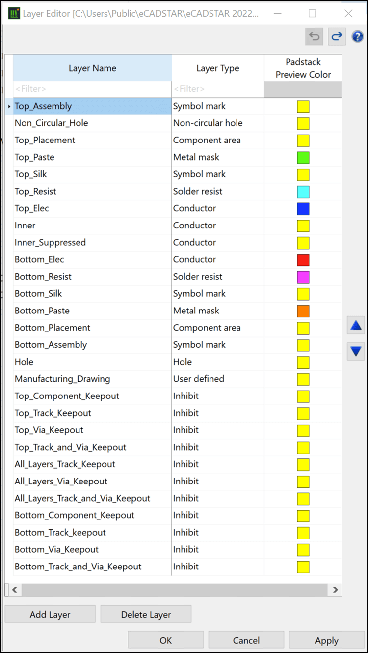
Footprint Layers
There is only one set of footprint layers in an eCADSTAR library. This master layer set is not a layer stack, and there are no materials or thicknesses at this stage – just the names of each layer, their layer types, and their padstack preview colors.
You don’t need a layer for every final PCB layer. If you did that, you would restrict or complicate how you use these layers elsewhere. To work efficiently, keep this set to the minimum you need.
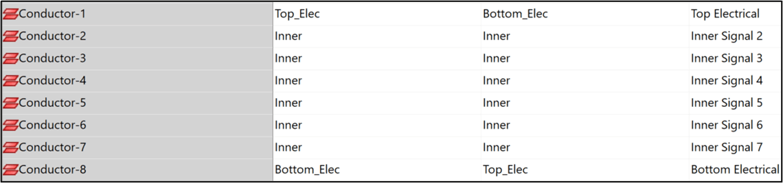
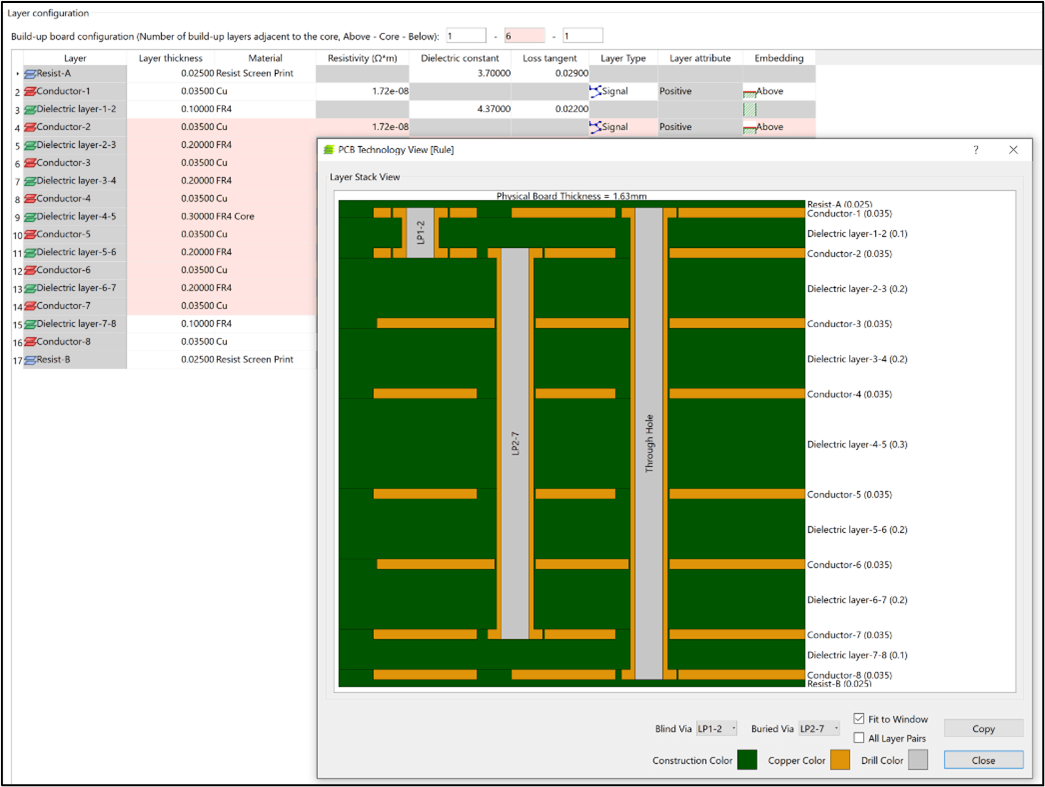
PCB Technologies
Each PCB Technology includes a set of layers you will use in a real layer stack, but still without materials or thicknesses. Taking a slice of an 8-layer stack, you can see that these 8 layers map to just 2 footprint layers. You can map to the same set of footprint layers from any other PCB technology.
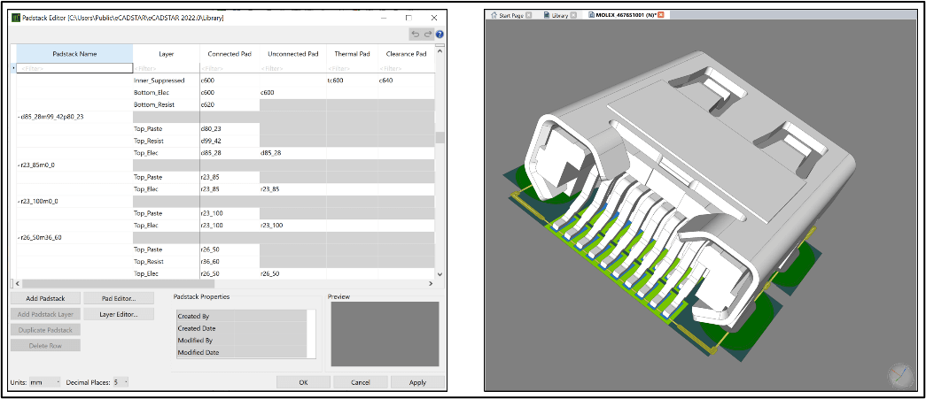
Padstacks
Like PCB technology, padstacks refer only to footprint layers, keeping these definitions as general-purpose as possible.
Since footprints reference these layers, they too are general-purpose. It’s easy to see what this means for parts in the master library, but what about parts you add from the Web?
For Web parts, the benefit is even clearer, because you only need to enter the absolute minimum information to get those parts working in your library. Padstacks in Web parts map to footprint layers, just like the ones in other library footprints
Once you have set up and saved layer mappings for an eCADSTAR Web components partner, it takes little more than a single click to add a part to your library.
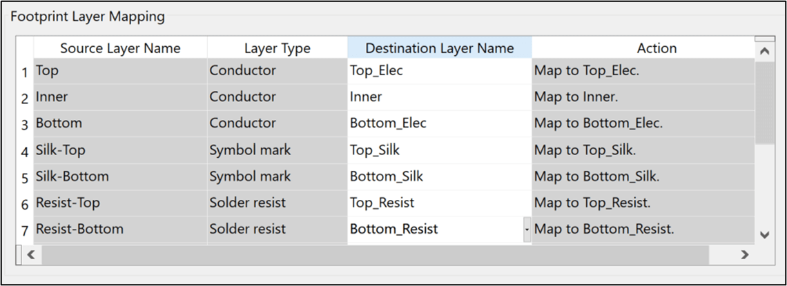
Since you map to a single, minimal set of footprint layers from padstacks, footprints, web parts and PCB technology, all these parts of your design data become re-usable and adaptable to the greatest extent.
Design Rules
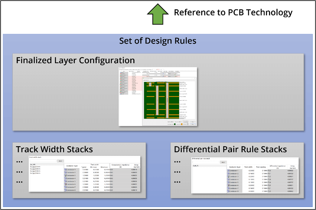
Design rules make your PCB functional and manufacturable. The same design rules apply to many different PCBs, or to parts of them, and that means re-use is key.
Each named set of design rules maps to a PCB technology. Following eCADSTAR’s re-use philosophy, multiple sets of design rules can map to the same PCB technology. In design rules, you add physical materials, thicknesses, etc. to create fully-defined layer stacks. These layer stacks often conform to those that are supported by your chosen fabricators.
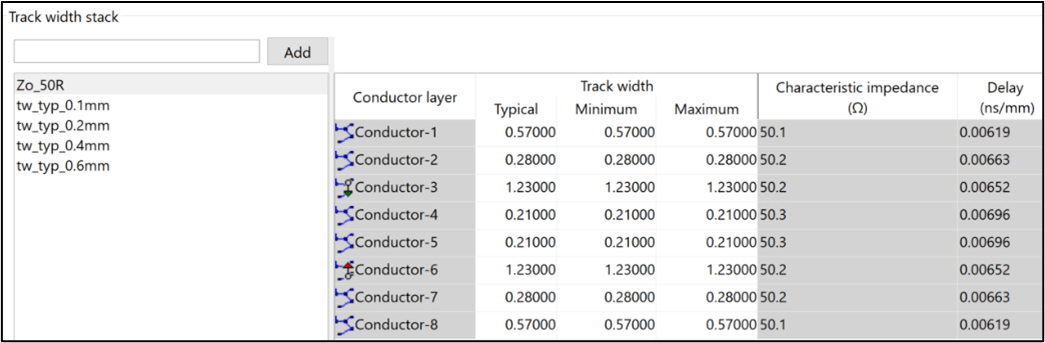
A track width stack describes the typical, minimum, and maximum track width for each PCB layer. Usually, you define multiple track width stacks that you apply to different kinds of signal and power routing, or to reference when you apply rules by area to specific parts of your PCB design, like fine-pitch BGA fanouts.
You can either enter the widths directly (sometimes specified by a fabricator) or calculate them here based on your desired characteristic impedance.
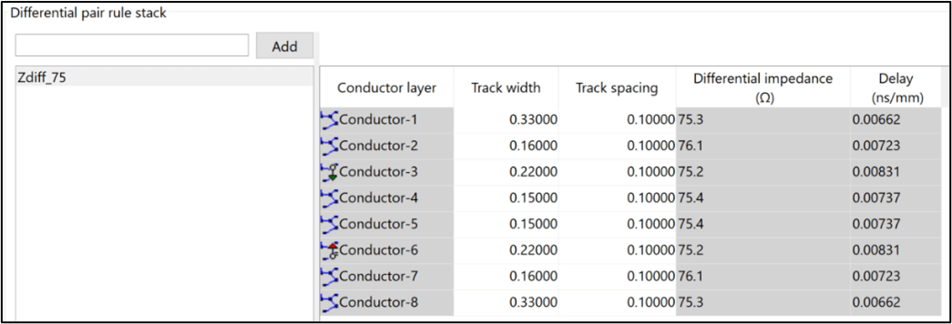
The same applies to rules for differential pairs, but here, the impedance is differential, and you need a differential spacing as well as a track width. This is because a (coupled) differential pair is one signal carried by two conductors, rather than two signals. This spacing is part of the structure of the pair, so it has to be treated separately from other spacings.
Each set of design rules includes one or more track width stacks or differential pair rule stacks and one or more sets of design rules map to each PCB technology. This structure means you minimize repetition. eCADSTAR also helps you adapt design rules. For example, if you add some PCB layers, width and differential pair rule stacks adapt to the change, so you only have to enter rules for the new layers.
Clearance Rules
Gone are the days when 2D clearances were sufficient for PCB design. Electric current follows the shortest electrical (not necessarily physical) path in all three dimensions.
As well as classic clearance rules, we must deal with creepage. That becomes more of a problem when there are high voltages. High voltages are much more likely to appear on mixed PCBs than classic all-logic boards. Components like avalanche diode arrays have many uses, including in automotive LIDAR, and they work at high voltages.
I=V/R so if V is high, significant current still flows even if R (say, the insulator surface of your PCB or the inside of a non-plated slot) is also high. And insulators don’t insulate so well when they get damp or contaminated.
So, while clearances are expressed in physical terms, creepage rules relate to voltage differences and materials, and this is how industry standards are defined.
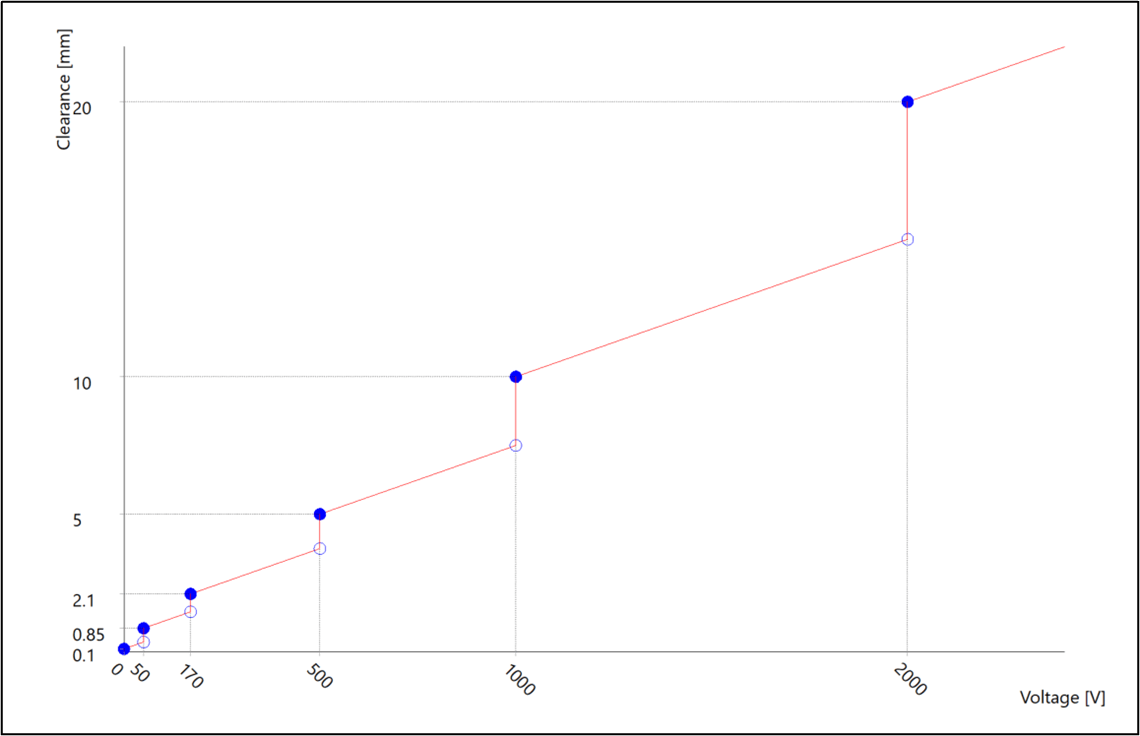
Here is an example. You can not only express clearance in mm, but also as formulas that relate it directly to voltage difference. That gives you more dynamic results. The lines in the graph connecting subsequent values of voltage difference and clearance become sloped rather than flat. This more dynamic assessment can make the difference between needing an engineering change or going straight to production.
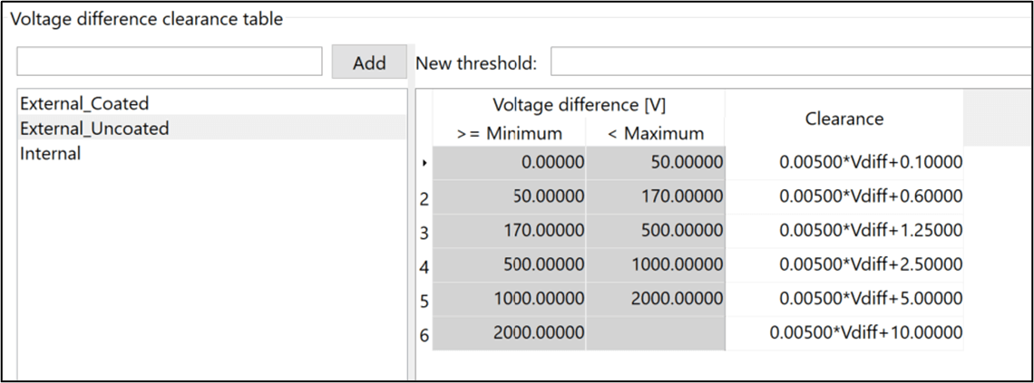
Other clearance rules are structured as rule stacks in the same way, and they all offer the same flexibility, with everything in one place and no repetition.
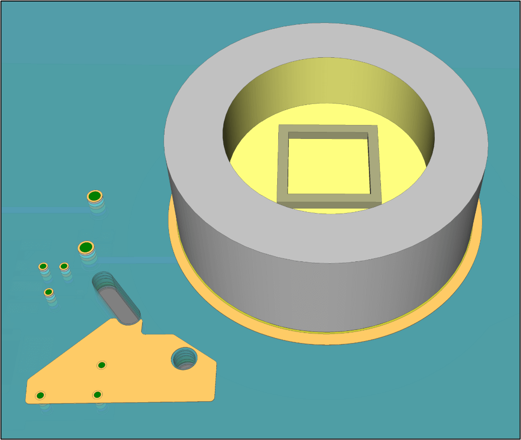
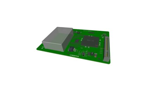
Managing 3D Models
You can import 3D models into your library from any source you choose. Some of them are unique to parts while others are multi-use. As with other parts of your library, to work efficiently, you must avoid repetition and organize clearly, while keeping your data as general-purpose as possible.
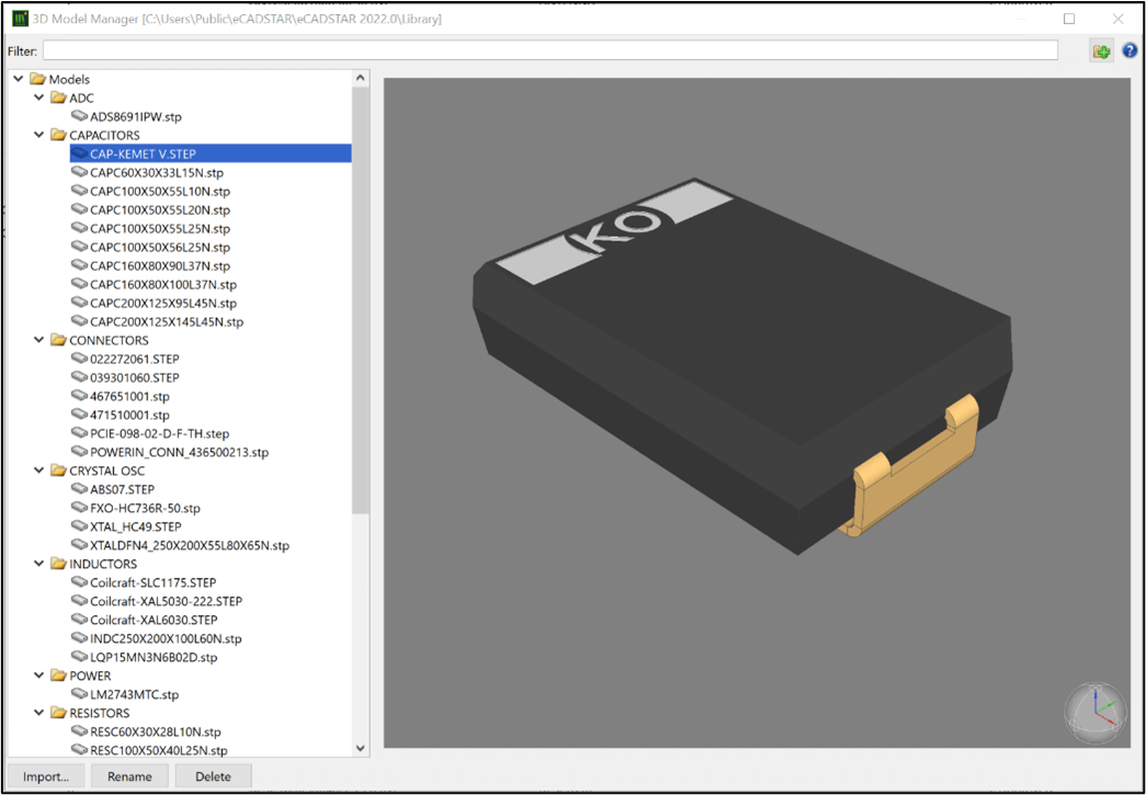
3D models are referenced by part footprints, but they are not embedded directly within them. This structure adds even more scope for flexibility and re-use. You can organize models into folders and subfolders in any way you choose. You could, for example, decide to group passive components into resistors, capacitors, and inductors, and within those definitions, into package dimensions. But equally easily, you could arrange them according to internal company definitions or standards if that suits your process better.
A 3D model can be unique to a single part footprint, or it can be referenced by as many part footprints as you like.
Summary
If you are creating or adapting an eCADSTAR library for the first time, I hope you find some of what I’ve said here useful. Every engineer has their own preferred methods and knows best what they need.
If I were to express one key takeaway in one sentence, I would say, “When you enter eCADSTAR library data, make sure it is general-purpose, to make downstream work faster and more reliable”.

-
Jane Berrie•Signal Integrity Expert, Zuken Tech Center, BristolJane Berrie has been involved in EDA for PCB signal integrity since the 1980s. Her articles have appeared in many publications worldwide - too many times to mention. Jane is also a past session chair for 3D IC design at the annual Design Automation Conference. Jane’s also an innovator with a unique perspective, who constantly works on new solutions in the fast-evolving world of electronic design. In her spare time, Jane has organized themed charity events - including two in aid of lifeboats and red squirrel survival. Jane is also a regular disco-goer.

- Blog

- Blog

- Blog
Discover how Quadra Solutions won the prestigious award and what it takes it win!
- Blog
Read more!