
CADSTAR Power Integrity Advance - Datasheet
TOP FEATURES AND BENEFITS
- Ensure quality and integrity of the power distribution system during and after layout
- Provide full board EMC screening for differential and common mode boardlevel EMC effects prior to production of the first prototype
- Accurate modeling of copper shapes for power delivery and noise transmission
- Simulate power distribution impedance profile over frequency and crosstalk hotspots for common mode noise
- Save cost and board space by reducing the number of decoupling capacitors
- Improve decoupling by determining correct distribution of capacitor values
- Indicate quality of placement location, value and trace/via connection
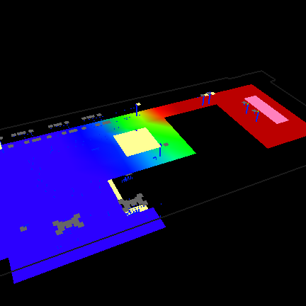
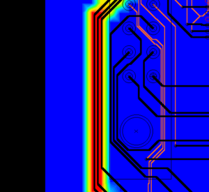
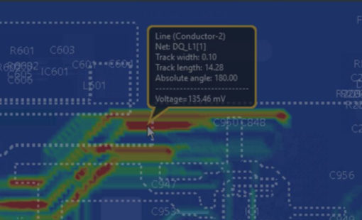
- Provide a clear graphical display of voltage and current distribution map for voltage drops and excessive current density
Introduction
Complexity of today’s design includes the growing counts of voltages, increasing switching currents from components, and more power consumption. This makes the study of power integrity a vital part of the design flow. Analyzing the performance and EMC behavior of your electronic design requires not only taking into account the design of the circuitry and geometry of the layout, but also includes the quality of the power distribution system. Parasitic noise voltages on the power/ground system is caused by integrated circuit (IC) gate switching inducing a switching current that can lead to malfunctions and significant increases in electromagnetic emissions.

High-speed designs utilize numerous high pin-count ICs, like FPGAs and CPUs operating on multiple voltage rails and strict signal noise margins. Take into account the complex split planes to support these IC’s, identifying voltage drops within a power supply due to losses in copper has become a necessity. As these IC’s become more of a commodity in electronics applications, the fight for the board space required to successfully transmit signals gets more aggressive. Careful design of the power distribution system is now a critical state in the
design flow.
CADSTAR Power Integrity Advance provides fast and practical power integrity and electromagnetic interference analysis within the real-time PCB design flow. With EMI, AC and DC power analysis combined in a single environment, you can determine the best decoupling and power distribution strategy for your pre-layout and post-layout stages with support for a complete what-if environment.
AC Analysis
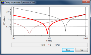
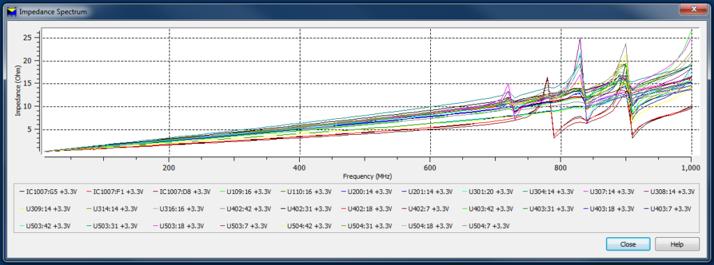
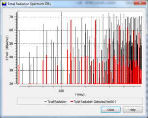
AC Analysis within Power Integrity Advance verifies plane impedance characteristics to assist the design engineer in the planning and selection of the decoupling capacitor network. The AC Analysis Engine verifies frequencydependent power impedance across the PCB to check if the supply impedance at a device is low at key frequencies, such as at a clock frequency and its harmonics.
High impedance may require corrective action such as placement changes, modifications to the decoupling network or reshaping of a power or ground plane. With Lightning Power Integrity Advance tightly integrated to the PCB design flow, you can make necessary changes concurrently and verify that IC vendor requirements are fulfilled.
DC/IR-Drop Analysis
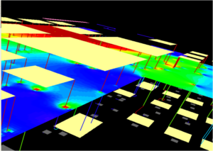
distribution network and its vias
CADSTAR Power Integrity Advance lets you conduct DC Analysis to identify unintended design behavior that impact the quality of power distribution and may cause the voltage supply to fall below specification at the target device.
DC Analysis automatically creates an equivalent DC circuit representing the power distribution system that is combined with model information of device power consumption to verify DC voltage drop (IR-Drop) and current flow. Common problems that can be identified include dense grouping of via holes causing increased local resistance.
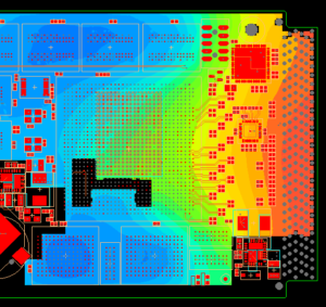
EMI Analysis
aggressor nets
EMI analysis in Power Integrity Advance highlights design behaviors that cause electromagnetic emission hotspots, considering both Common Mode and Differential Mode radiation for nets, connectors, and other PCB elements. Engineers can easily cross-probe critical nets to layout and make immediate changes or conduct what-if analysis with routing, component values, and copper areas to achieve optimal results.
The EMI analysis module includes a trusted research-based algorithm developed by Zuken in collaboration with the EMC Expert System Consortium at the Missouri University of Science and Technology. The algorithm was designed to ensure fast and meaningful EMI results to assist in creating reliable PCB designs.
 Power Integrity Advance – Datasheet
Ready to brush up on something new? We’ve got more to read right this way.

- Solutions
Aggiornamento dei progetti CADSTAR a eCADSTAR
- Pagine
È facile non accorgersi di un serio problema di integrità dell'alimentazione o di EMI.

- Schede Tecniche
I controllori configurabili, i sensori, l'Internet of Things (IOT) e molte altre tecnologie richiedono un'attenta distribuzione dell'alimentazione. I problemi possono facilmente sfuggire - non solo DC, ma anche problemi sottili che coinvolgono l'accoppiamento elettromagnetico.