
Rule Areas Help You to Design Reliable, High-Density PCBs
Different neighborhoods need different rules
Some kinds of infrastructure work the same way in all areas, partly because making them all different costs too much. The more specialized activities become, the more they need their own areas, where the environment suits them. Last weekend, my fiancée and I visited a wetland bird sanctuary. A very good area of land for that attraction, but not a good place to build a town unless the buildings are on stilts.
And there are more specific rules to follow for each part of the sanctuary. There are lakes for ducks, reed beds for reed warblers, shallows for wading birds and so on. And there are pathways between and through them for visitors, to keep their feet dry.
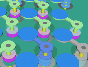
A mixed-technology PCB is created on similar principles.
Routing guidelines, best practices and topology control all make PCB layout design faster and more reliable, but PCBs often comprise many circuits, each with their own requirements. This trend becomes ever stronger with higher density and inclusion of specialized chipsets and sensitive circuits like RF antennas and buck converters.
Differences in design rules can apply to different PCB areas in both the XY plane and on the Z-axis.
Layer stack
Layer stacks are usually uniform in terms of insulating and conducting layers, but not necessarily in terms of what is on those layers.
A high-speed area may need more reference plane areas above or below in the layer stack to control impedance. Those areas can be drawn as template shapes that adapt to routing changes.
High-Density Interconnect (HDI) layers can be added on the top or bottom of the PCB, so that much smaller vias can be used under fine-grid components, providing more routing channels in and out of devices and lower parasitic inductance and capacitance. The improvement in density that such layers allow may offset the extra cost.
HDI layers cover the entire board surface, but inner layers can be used for different purposes and microvias that connect between HDI layers are only used where you need them.
Rule areas: single-ended and differential track width and spacing
You can control both single-ended and differential rule stacks by rule area, and then apply those rules to either all layers or specific layers.
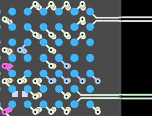
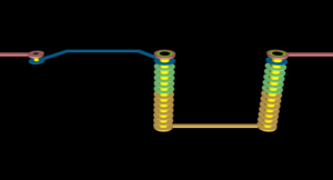
Getting routes in and out of fine-pitch BGAs (FBGAs) can be challenging, especially when dealing with differential pairs. You cannot simply split a modern, fast differential pair at the device boundary, because you have to maintain not only length matching but electrical behavior, including differential impedance. And there are many more differential pairs than there used to be, because they are so much better at carrying very fast signals.
The usual way to get a differential pair between tight-pitch pads is to neck them down while maintaining the impedance. Tracks have to remain parallel and coupled at the right spacing until they almost reach their pads.
Keeping track with and differential pair spacing at full size elsewhere enhances reliability.
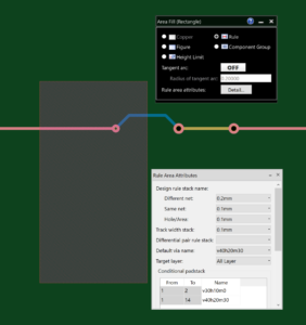
In guides like this one from Xilinx, 0.08mm track width and track-to-pad spacing are recommended for differential pairs in the FBGA area.
I set two differential-pair rule stacks for the top layer: one for standard parts of the routing and one for necking down into the FBGA. I did this in the local rules for the PCB, but I could equally have done the same in the library design rules. The calculated differential impedance is around 85Ω in both cases – a common desirable target differential impedance for signaling like PCI Express (PCIe) and memory clocks and strobes.
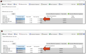
The spacing rules for the FBGA shown below are so tight that there is no leeway at all. To achieve 85Ω, the BGA pads can be no bigger and the track widths and differential spacing have to be exact. This forces a very useful cross-check, because if any of these are even a micron out, and checks are enabled, PCB Editor will not let you route the pair between the pads.
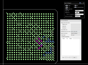
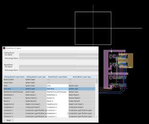
Rule areas: via type and via span
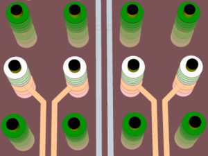
You can control default via padstacks and conditional padstacks. Conditional padstacks control which vias are used within which layer spans. If you had, say, two high-density-interconnect (build-up) layers at the top of the layer stack, you might decide to make tiny, laser-drilled vias the default between those two layers in high-density areas, but not, for example, within the layout areas of power supplies, where you need bigger vias for low-resistance connections.
Some fine-pitch devices relieve you of the need to neck down differential pairs, by placing them only on pads at the periphery, but differential signaling is so common that this isn’t always possible. In fact, on some devices, surrounding pads are grounded to create a controlled-impedance path through the layer stack in the Z-dimension. In this example, it’s easy to see that if a high-density layer pair were used in place of the through-hole vias, then both the signal and grounded vias would span only two of the PCB layers.
Final thoughts: re-using board blocks and their rule areas
I always find it useful to think about how one feature makes another more powerful, and rule areas are no exception. In PCB Editor, you can export Board Blocks—parts of a PCB layout—and re-use them in other designs. If the areas you export contain rule areas, they get re-used too, so you can apply the same rules, or different ones, to the same areas.

-
Jane Berrie•Signal Integrity Expert, Zuken Tech Center, BristolJane Berrie has been involved in EDA for PCB signal integrity since the 1980s. Her articles have appeared in many publications worldwide - too many times to mention. Jane is also a past session chair for 3D IC design at the annual Design Automation Conference. Jane’s also an innovator with a unique perspective, who constantly works on new solutions in the fast-evolving world of electronic design. In her spare time, Jane has organized themed charity events - including two in aid of lifeboats and red squirrel survival. Jane is also a regular disco-goer.

- Stampa
Aprile 30, 2025
eCADSTAR 2025.0 Release
Click Here!
Read now
Le nuove funzionalità semplificano la gestione delle librerie, aumentano la precisione nei progetti “high speed” e ottimizzano la documentazione ...
- Pagine
Aprile 23, 2025
SOFTWARE LICENSE AGREEMENT - eCADSTAR Design Viewer
- Products
Aprile 08, 2025
Novità di eCADSTAR 2025.0
Key highlights sulla versione eCADSTAR 2025.0
Read now
L'aggiornamento 2025.0 ti consente di soddisfare la crescente domanda di progetti elettronici compatti, ad alte prestazioni e a basso consumo energeti...

- Blog
Gennaio 31, 2025
High-Speed SerDes Channels and Overcoming Physical Effects for Optimal Performance
Blog
Power integrity is a critical stage of successful PCB design. Employing a diverse range of strategies and tools is essential for any designer.