
Design Variation and Block Hierarchy for Versatile Re-Use
What are Multi-Instanced Block Hierarchy and Design Variation?
Multi-instanced block hierarchy comprises the ability to:
• Define parts of a schematic as blocks that can be used multiple times, by adding instances of those blocks to a schematic sheet
• Create hierarchy within block definitions so that a definition can include multiple instances of another
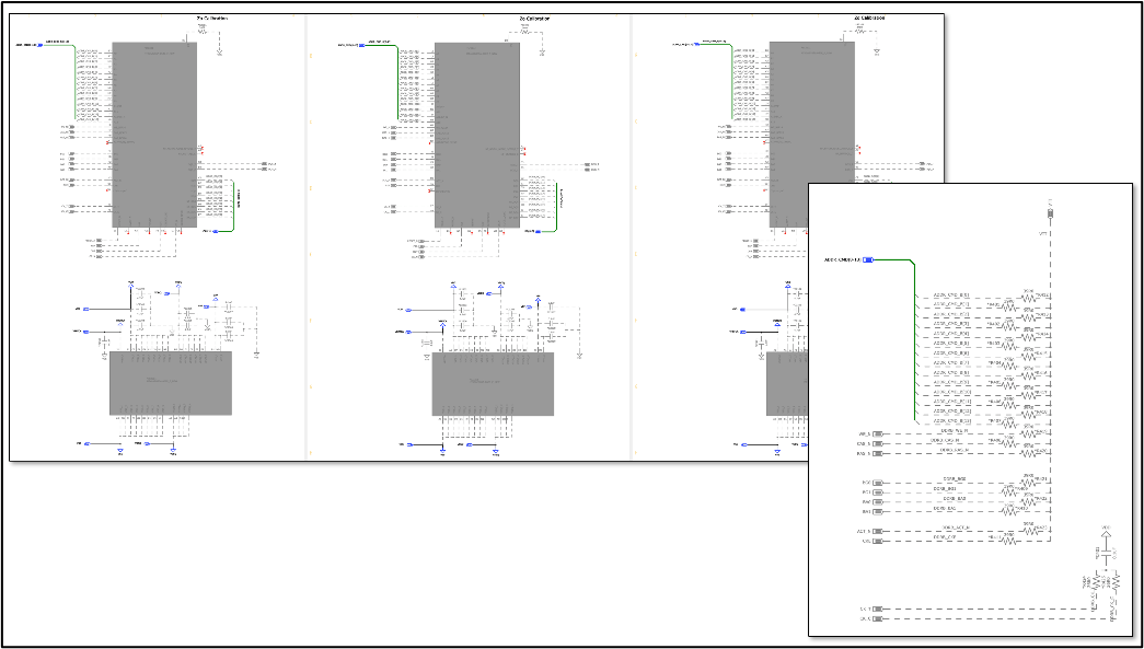
It’s probably easier to visualize this as a diagram. Figure 1 shows the block definition hierarchy I used for the DDR4 circuit in my previous blog, as seen in eCADSTAR.
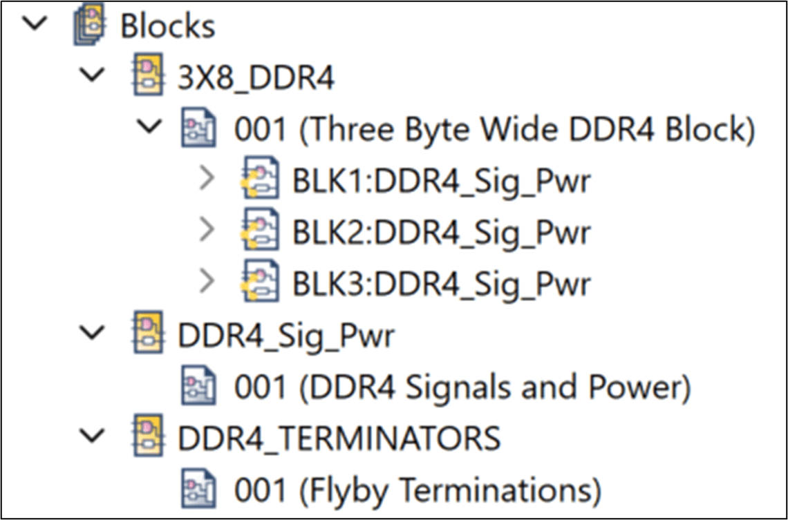
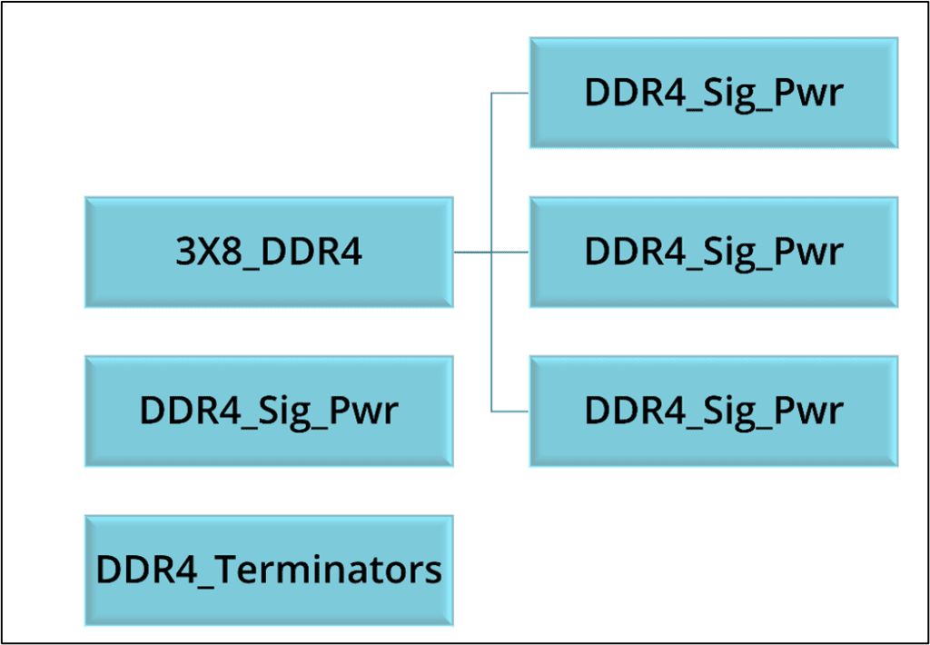
Figure 2 shows the hierarchy of block definitions in a more visual way. You can use multiple instances of each of these block definitions independently in your schematic designs. If you create instances of 3X8_DDR4, then each of those include three instances of DDR4_Sig_Pwr. If you make a change at any level in these block definitions, it can ripple through the hierarchy to update every instance, but if you’re implementing an ECO, it pays to be more selective.
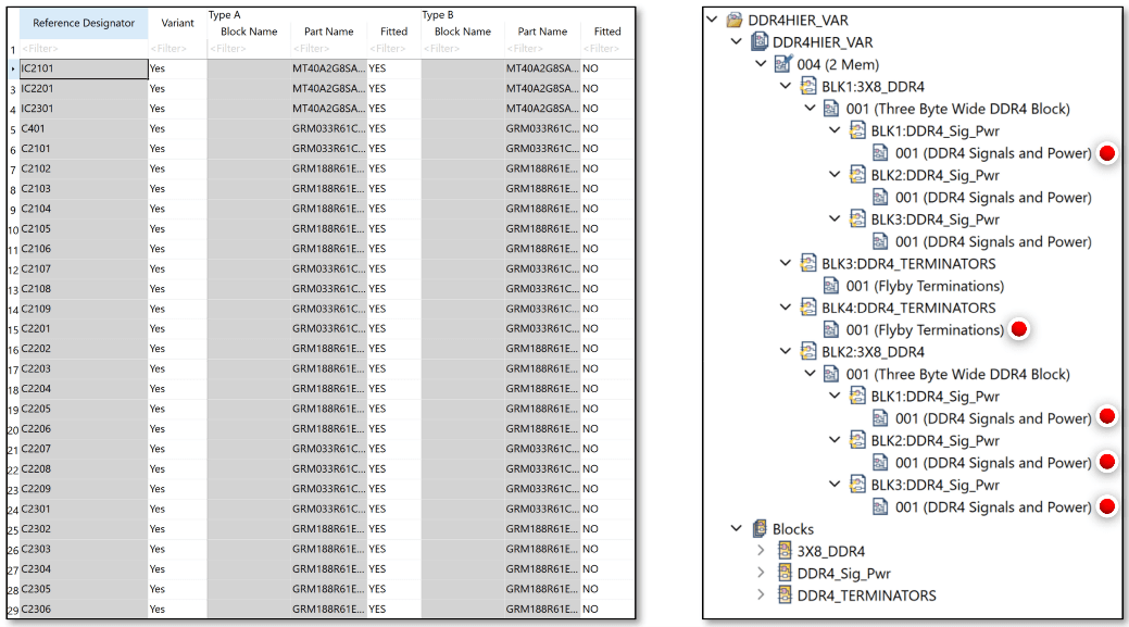
With variation management, you can decide which parts get fitted in which variants on the same bare board, and even which parts are used in each variant when fitted. This is particularly useful for parts like memory chips, where there are different varieties with the same PCB footprints.
At the top level of this schematic (Figure 3), there are two instances of 3X8_DDR4, each connected to an instance of DDR4_Terminators. That makes it easier to see the structure, and it also makes it easier to create design variants, because the contents of blocks can be variant components.
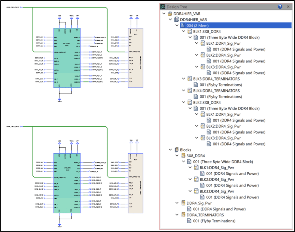
After opening the schematic sheets underlying these blocks, and setting which are fitted (Figure 4), there are now two variants, Type A and Type B. In Type B, one of the memory blocks is omitted, but the bare PCB remains the same.
eCADSTAR Schematic Editor shows what is and is not fitted in each variant by shading components and drawing net connections with dashed lines (Figure 5).
How Does Schematic Block Structure Relate to PCB Design?
Schematic blocks do not transmit directly to PCB design. There is no need. PCB blocks do not have to correspond directly to schematic blocks, and this gives more flexibility, because PCB blocks can be created, saved, and re-used, completely independently. I won’t cover that in this blog – I’m saving that for another,
Variant structure is reproduced in PCB design, because it reflects which components are fitted, and if those settings correspond to the block structure, variation is easier to manage.
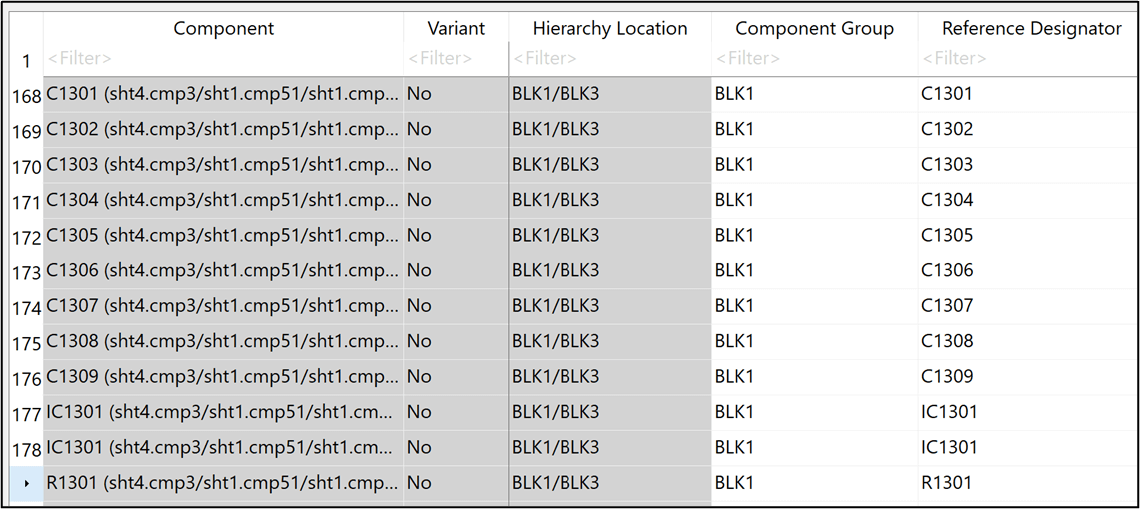
In cases like this memory design, however, there are also benefits in relating schematic block structure to components in the PCB design. The easiest way to do that is to create Component Groups. In this case, I just assigned Component Groups according to top-level block instance (Figure 6).
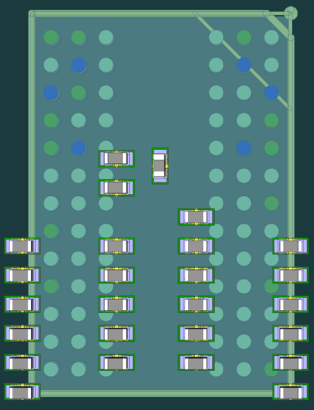
• BLK1 and BLK2: Groups of three DDR4 memories and associated components
• BLK3 and BLK4: Groups of terminators for BLK1 and BLK2 respectively
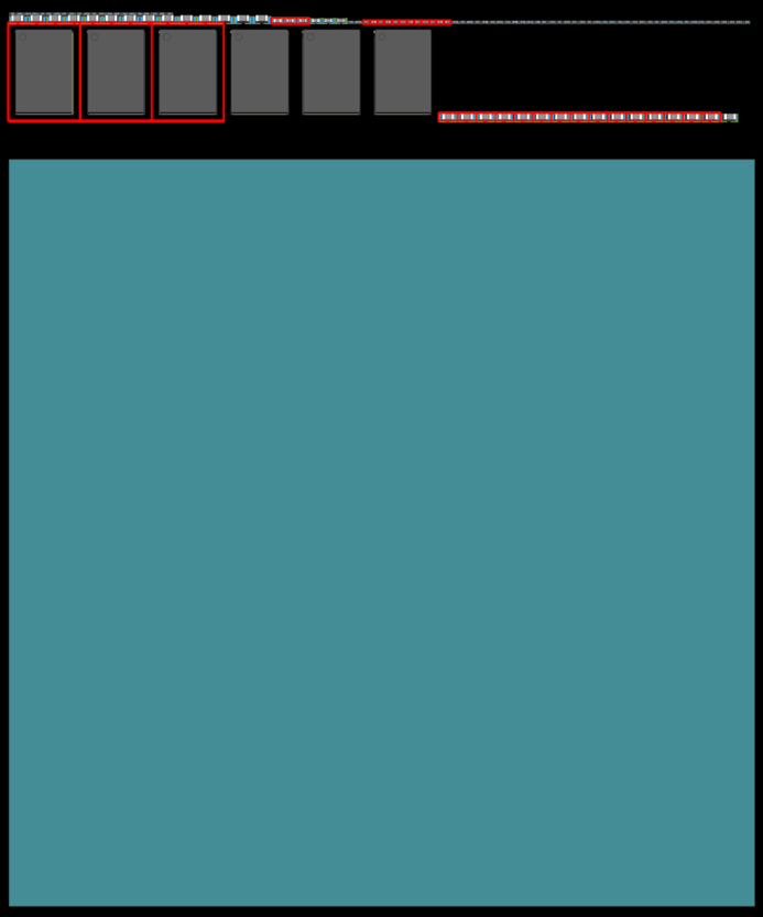
Now it’s easy to highlight, select or filter any of these groups in PCB Editor, for example BLK1 (Figure 7).
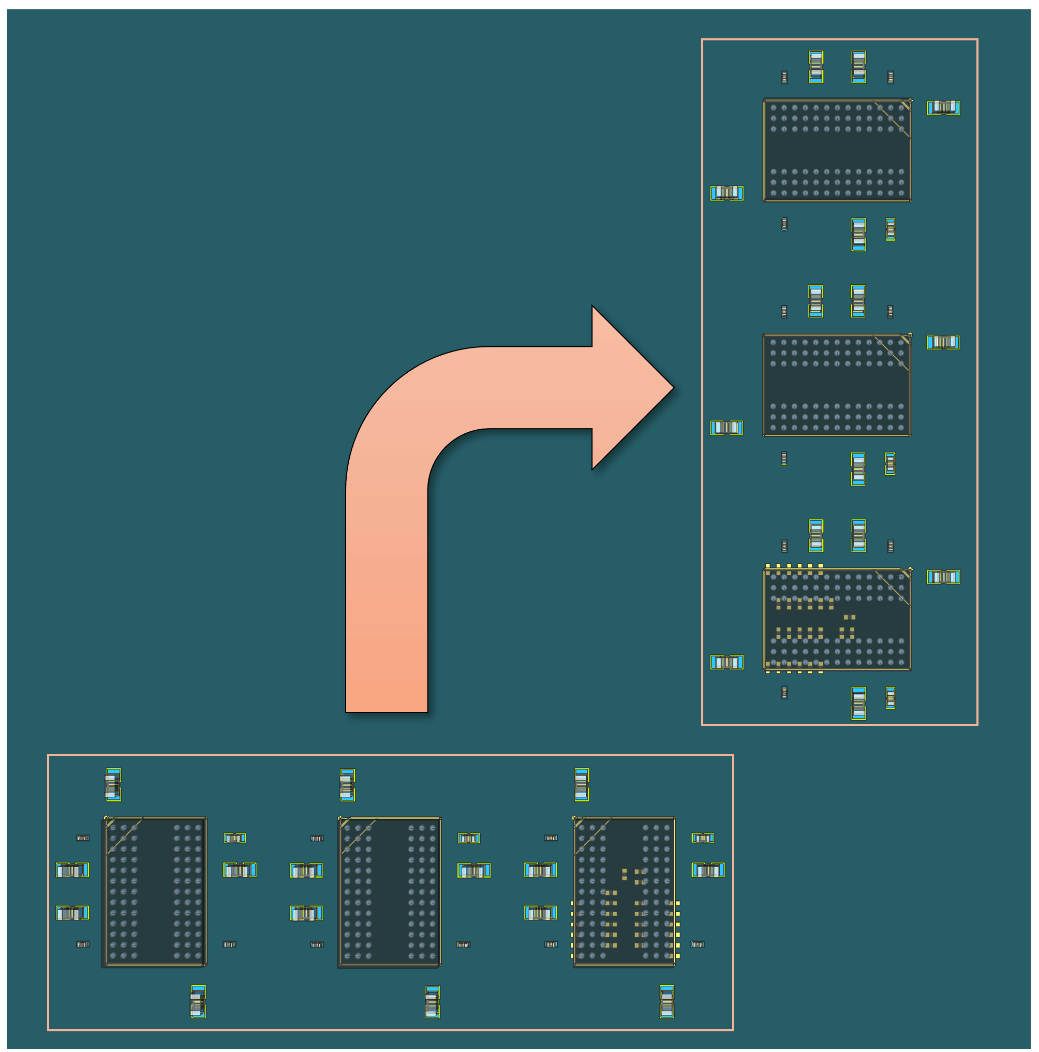
Now for some re-use. The arrangement of local decoupling capacitors is the same for every memory chip, Firstly, I re-used a similar placement for one chip and its capacitors from another design, by exporting the positions and mapping them to components in this board.
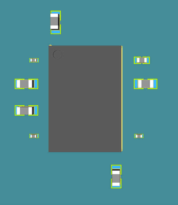
Then I used Copy Placement in PCB Editor to replicate these positions on the other two devices in a set of three. I replicated terminator placement on the final device in the Fly-by topology chain by re-using their placement from the other design in the same way.
In the schematic, I added different increments to reference designators for each instance of the same block. That strategy makes replication mappings much easier, and often completely automatic. It is easy to see, for example, that IC1 in a block definition maps to IC1101 and IC21011. This regularity means the initial mapping order PCB Editor presents to you is usually what you want.
Replicating and re-orienting relative placement for the entire memory bus to create one that corresponds to the second block instance in the schematic took only a few seconds.
Summary
Regularity in schematic block hierarchy not only makes ECOs much more straightforward but also does the same for placement re-use. I did not show routing re-use here but copying routing from one circuit to its replicant is a simple copy/paste.
Regularity like this is a form of symmetry, and symmetry is good for consistency. When identical circuits are, as far as possible, laid out identically, there are fewer ways for things to go wrong unexpectedly in production hardware. That is especially true for layout-critical circuits like these.

-
Jane Berrie•Signal Integrity Expert, Zuken Tech Center, BristolJane Berrie has been involved in EDA for PCB signal integrity since the 1980s. Her articles have appeared in many publications worldwide - too many times to mention. Jane is also a past session chair for 3D IC design at the annual Design Automation Conference. Jane’s also an innovator with a unique perspective, who constantly works on new solutions in the fast-evolving world of electronic design. In her spare time, Jane has organized themed charity events - including two in aid of lifeboats and red squirrel survival. Jane is also a regular disco-goer.

- Blog
Jane Berrie teaches you how to use the eCADSTAR Library Editor and to re-use design data effectively
- Video Library
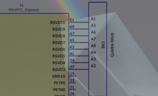
Hierarchical blocks are normally used for top-down designs, where the block is drawn on the top-level schematic and associated signal pins are added.

- Products