Instant Web and Local Parts
Save time when you prototype, even before your new components are in your library. Download what you need and carry on working. Search for a part and it appears on your cursor. Drop it and it becomes part of your PCB layout.
Web part lookup gives PCB engineers access to extensive online parts libraries, including 3D models.
Native 3D and Simultaneous 2D/3D PCB Design Editor
2D or 3D viewing—which is best? To avoid DRCs while placing components, usually 3D PCB design. And with fast signalling, the third dimension comes into play. But when you’re routing, working in 2D provides more focus on routing topology and patterns. So why choose when you can have both? You can split the view and route in 2D with simultaneous 3D display.
Additionally, your 3D canvas can include both PCB and enclosures. You get ahead, detecting issues like component-to-enclosure collisions right on the canvas.
Native 3D design means collisions and DRCs get detected early—often in real-time, during the interactive layout of the PCB. Another great feature is simultaneous 2D/3D design. It gives you the best of both worlds—for example routing a critical differential pair in a familiar 2D view while seeing how it relates to other objects in 3D.
Board Blocks
Board Blocks equip you for maximum re-use, design integrity and teamwork. Once you create a block and make it a child board, you can re-use it anywhere on your PCB design. Furthermore, you can work on blocks independently and merge or re-merge them intelligently into your designs. You can even create your own library of physical design blocks and share with whoever you wish.
Board Blocks are parts of a PCB design that you identify and save as re-usable work. If you identify a Board Block as a Child Board, then you can re-import it at any time to reflect engineering changes (ECOs)—even if other engineers have worked on it. For example, you may have a colleague who is particularly good at optimizing power supply layout of your PCB, so you can re-import later without interrupting your work on the main PCB design.
Design PCBs With Superb Interactive Routing
At the heart of eCADSTAR’s PCB design software is its highly configurable yet straightforward interactive routing.eCADSTAR recognizes that signals take many forms and our PCB layout platform works with you to get them connected as neatly and effectively as possible, considering all the intricacies of today’s PCBs.
Denser and denser routing carries faster and faster signals with more and more mixing of analog, digital, power, and RF. Our PCB design Editor was designed to handle all that, with the help of your skill and experience.
Optimize PCB layout with efficient interactive routing with control where you need it. Interactive routing follows guidelines you can configure, helping you conform to best practices.
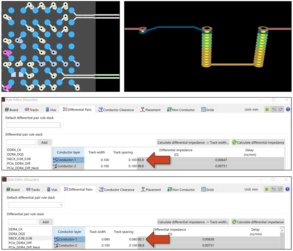
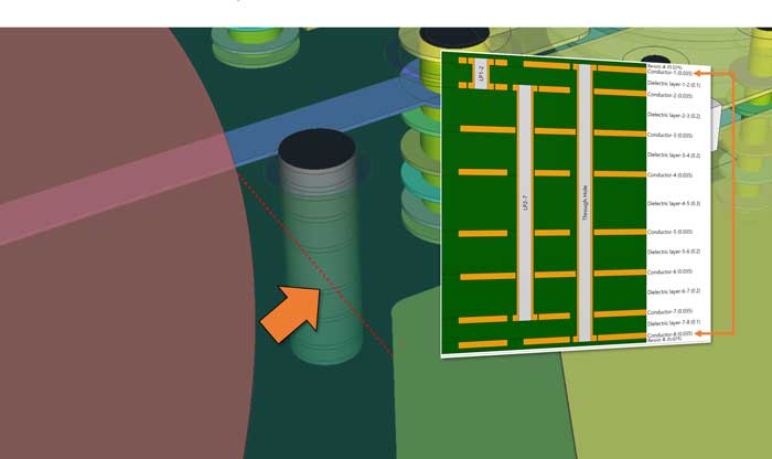
High-Speed PCB Design
With eCADSTAR’s PCB design software, high-speed design is built-in, not an afterthought. It goes as shallow or as deep as you need. Yes, topology control, impedance control, simulation and power integrity analysis when you need them, but advanced re-use features also make high-speed design much faster and safer.
Some high-speed features are cost options, so you decide and pay for only what you need.
Control high-speed layout of PCB without external software in a consistent, unified environment: Topology, impedance, crosstalk, signal integrity, and much more.