Overlooking a High Speed Circuit Creates Signal Chaos
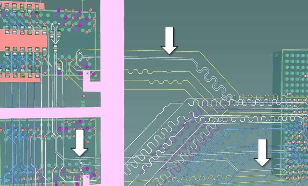
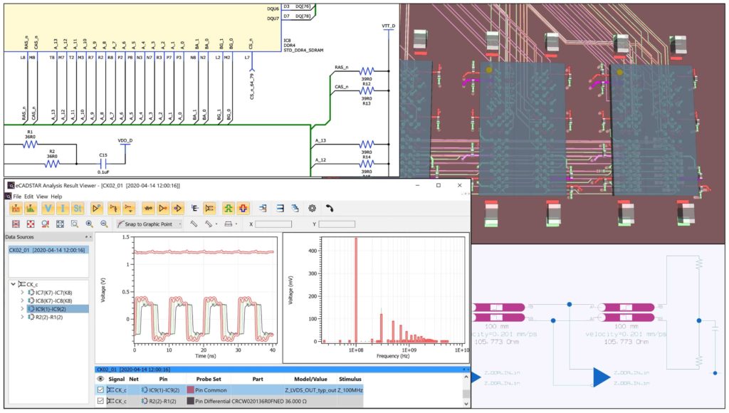
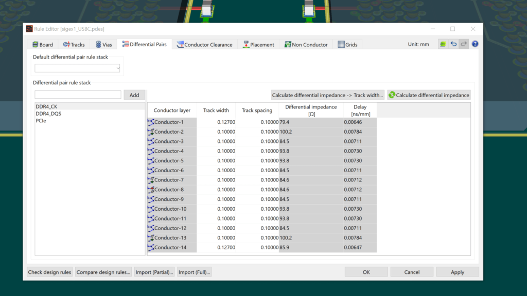
You have to design the routing topology of your high speed PCB carefully—trace geometry, layer stack, materials and electromagnetic coupling—or else signals will be degraded or dysfunctional.
This can apply to any part of a circuit board. Many standards, including the commonest memory circuits, PCI Express and USB, require high speed PCB layout and routing.
Selected areas—or even signal layers—of a PCB, often must be treated as high-speed, even if the rest of the PCB does not.
High speed board design means concern for signal integrity. Treating high-speed signals as travelling waves. Making the paths they take as smooth as possible in electrical, not just physical, terms. You can optimize your PCB design for maximum resilience, going beyond basic design rules and guidelines such as trace length, trace width, and component placement.