IS YOUR PCB LAYOUT HIGH-SPEED?
Even using standard components like DDR3, DDR4 or DDR5 SDRAMs means following high-speed PCB design guidelines. Let’s route some DDR3 memory.
IS YOUR PCB LAYOUT HIGH-SPEED?
More and more PCBs combine multiple circuits. Your PCB doesn’t have to clock at gigahertz to be high-speed – and to add to that, technologies like IOT and smart home controllers are growing exponentially.
Even using standard components like DDR3, DDR4 or DDR5 SDRAMs means following high-speed PCB design guidelines. You need to constrain your PCB layout to achieve top-class signal integrity – so it works properly – but also so your product is the best it can be.
eCADSTAR isn’t the only solution that lets you do that. The difference is in the way it’s all built-in, not an afterthought – and its unrivalled ability to work with the complex detail you need for ultra-critical layout.
But before we delve into details, what key high-speed constraints do you need?

High-Speed Signals Need a Smooth Journey
IMPEDANCE
All high-speed PCB signals are impedance-controlled. Without impedance control, high-speed signals run wild and random. Standards and application notes often specify the impedance you need to achieve. For example, PCI Express (PCIe) Generation 3 works well at 100Ω differential impedance, while for DDR3 and DDR4 memory, 45Ω to 55Ω single-ended impedance is often recommended.
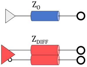
Zo and ZDIFF are Fundamental to High-Speed PCB Design
In eCADSTAR, you can constrain both single-ended and differential impedance. eCADSTAR can derive the track widths and differential spacings you need to meet your constraints on each board layer and check that your design has met them.
LENGTH, DELAY AND SKEW
When you route a signal from point to point on a single layer, delay generally runs with length – and length is easier to work with. Length is concrete and visible. Length is often what’s specified in standards and application notes too.
But add branches, vias and width changes – maybe coupling to other tracks – and you need to work with delay.
eCADSTAR works with both length and delay, including built-in simulation that drills down to whatever level of detail you need, including effects like signal-to-signal coupling.
Once upon a time there was a master clock and all the logic latched to its beat. These days, most logic is source-synchronous. You route groups of signals with their strobe. You need to constrain relative delay or length – also called skew. In eCADSTAR you can constrain skew and see that your design is within constraints as you route.
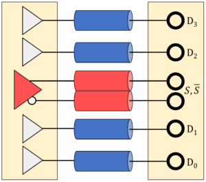
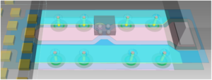
Data Bits Matched to Their Differential Strobe
TOPOLOGY & HIGH SPEED PCB DESIGN
Topology is the way routed connections are arranged in electrical terms. Topology templates show what the routing should look like when it is converted to a transmission-line equivalent circuit, because this equivalent circuit is what the travelling signals “see” as they travel from source to load. Their topology describes the intersections, side-roads and waypoints on their journey.
In high-speed PCB design, signals always need a constrained routing topology. You’ll find similar advice for SDRAM, PCI Express, USB and other signals in many application notes as well as in applicable signaling standards, from sources such as JEDEC. In many cases, standards are free to download after registration.
eCADSTAR recognizes all this with a wide selection of templates and instant visualization that make topology control as fast and reliable as possible. You can also set length and impedance constraints in topology templates and apply them to as many signals as you like.
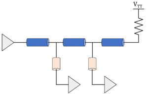
Singe-Ended Fly-By Topology
DIFFERENTIAL SIGNALS
More and more differential signals are showing up on PCB layouts. USB and HDMI I/O, PCI Express buses, DDR memory clocks and strobes and many others. Differential signals are popular because they can go faster – faster even than many electronic engineers thought possible decades ago. In eCADSTAR, differential signals get the special treatment they need, with automatic, clean end routing, specific design rules and constraints and instant copper-plough.
Differential Routing to Mid-Mount USB Type C Socket (eCADSTAR PCB Editor)
WHEN YOU NEED TO GET RIGHT DOWN WITH THE METAL
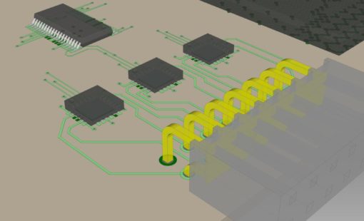
When it comes to really challenging tasks like this module-to-antenna routing, you have to be able to see exactly what you’re doing, with precise geometrical editing and versatile 3D view. If you have to switch applications, you can lose focus on what you’re doing. For example, RF signals need to be routed to tight 3D geometry requirements. In some cases, certification relies on it. So together with front-to-back high-speed constraints and layout, you need efficient shape editing, with fast automatic adaptation and plough-through. It’s all there to try for yourself in the eCADSTAR Discovery Release.
Routing from a Land Grid Array (LGA) to a Low Noise Amplifier (LNA) and Modular Satellite Tracking Antenna (eCADSTAR PCB Editor)
ONE WAY TO SET CONSTRAINTS MEANS YOU CAN DO IT YOUR WAY
eCADSTAR has a consistent user interface from design entry through physical layout, so the way you set constraints is the same, wherever you set them – in schematic or physical design or in library design rules.
To make your design process even more reliable, you can save many constraints as templates and constrain signals by applying those templates to them. For example, you can add node-to-node trace length constraints to topology templates and engineers can share them.
eCADSTAR’s consistent user interface runs much deeper than just constraints. Why should there be different ways to move or copy an object, just because you’re working with the library – or entering a schematic – or laying-out a PCB?
JOIN US ON A JOURNEY OF DISCOVERY
We know your time is precious, but we’d love to welcome you aboard, to try out the eCADSTAR Discovery Release for yourself – and discover what it can do to make your high-speed PCB design process a smoother ride.
There’s much more detail in CONSTRAINT-DRIVEN DESIGN. Please take a look.


- Press
May 06, 2026
eCADSTAR 2026.0 Release
Click Here!
Read now
New release enables faster design processes, easier data management, and improved handling of complex PCB projects.

- Products
February 19, 2026
What's New in eCADSTAR 2026.0
Key highlights of the eCADSTAR 2026.0 update
Read now
The 2026.0 release optimizes your workflow from design to library management, allowing for faster and more efficient execution.

- Press
November 11, 2025
Zuken-TME Partnership
TME brings real-time access to component availability, pricing, and ready-to-use EDA models directly into the eCADSTAR environment.
Read now
TME is expanding integrated services within Zuken’s eCADSTAR platform.
RELATED PRODUCTS
- Datasheets
August 07, 2019
PCB Editor Datasheet
PCB Editor, part of the eCADSTAR product, is a borderless electronic design environment. Has a part become obsolete? Then using the internet-connected platform, eCADSTAR Web Part Lookup allows you to rapidly search for an alternative and it will appear directly on your cursor with one click.
Read now
A layout tool that may be used to create board shapes, arrange components, define routing patterns and produce manufacturing outputs.
- Datasheets
August 07, 2019
Schematic Editor Datasheet
Schematic Editor, part of the eCADSTAR product, is an efficient and intuitive schematic capture application that may be used to define part connectivity, variation and design constraints for use in the eCADSTAR PCB Editor.
FREE DOWNLOAD
A schematic capture application that may be used to define part connectivity, variation and design constraints for use in the eCADSTAR PCB Editor.
- Datasheets
August 07, 2019
Library Editor Datasheet
Connect to your preferred part vendor directly from within the eCADSTAR Library Editor application to lookup part information such as stock, pricing and datasheets. Download parts, symbols, footprints and 3D models and merge them to your library instantly with automated layer and attribute mapping.
FREE DOWNLOAD
A comprehensive unified design resource creation and management interface – more than just a part library.

- Products
May 15, 2019
PCB Features
A flexible, modular approach allows you to build an eCADSTAR bundle to fit your pcb design requirements.
Read now
With a wealth of standard features and modular add-ons, eCADSTAR allows you to tailor your design bundle to meet your PCB design requirements.