Power Integrity analysis in PCB

Power Integrity and EMI

Causes can be subtle, but you can avoid a lot of PI and EMI trouble with eCADSTAR Power Integrity Analysis and EMI Analysis.
Menu

FAST EMC VERIFICATION

  • Fast EMC noise source identification with what-if capabilities.
  • Complete board EMC screening, and worst-case EM emission prediction.
  • Based on an industry-accepted R&D approach (UMR EMC Expert System Consortium).
  • Fast algorithms to analyze: Differential Mode Radiation (DM), Common Mode Radiation (CM), and Power Bus Noise (PB).
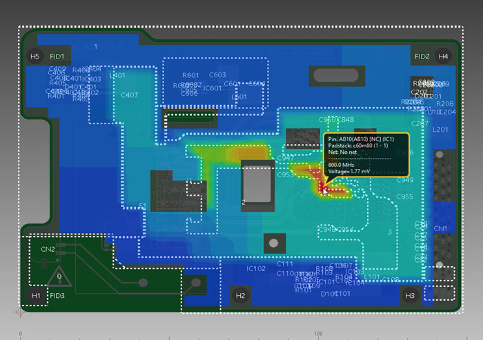
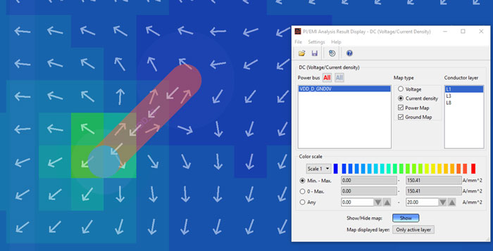
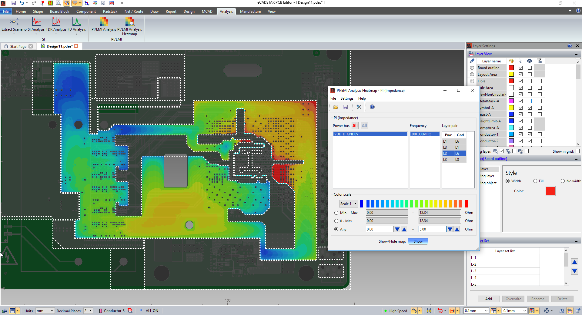
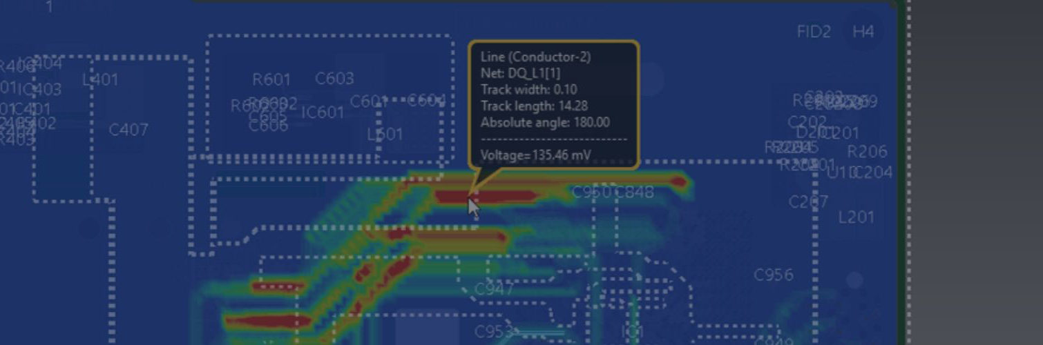
  • Display heatmap style EMI estimation results directly on eCADSTAR PCB Editor canvas.

Power Integrity Analysis in PCB

EMI COUPLING MAP

Power Integrity Analysis in PCB

DC VOLTAGE – PI/EMI ANALYSIS RESULT DISPLAY

POWER INTEGRITY ANALYSIS – DC 

  • Numerical frequency-domain solver (2.5D approach) for DC and IR-Drop analysis with user-controlled meshing density.
  • Allows analysis of arbitrary/irregular PWR/GND shapes.
  • DC voltages, IR-Drop, and Current Density.

DC SIMULATION – IC POWER-PIN VOLTAGE AND PDS VIA CURRENTS

  • Computation of the max current and the voltage drops of the PDN via’s.
  • Identify problematic vias, define thresholds for the maximum current flow allowed.
  • Parametric studies on PDN vias for what-if analyses.
  • Integration and cross-probing into eCADSTAR main canvas (2D/3D) pinpoints to critical board areas.
  • Calculation of the DC resistance (DC-R analysis) allows verification of IC manufacturer specifications.

Power Integrity Analysis in PCB

PI: VIA WITH HIGH CURRENT/STRONG VOLTAGE DROP (EXAMPLE)

pi impedance-map

PI IMPEDANCE

POWER INTEGRITY – AC ANALYSIS

  • Numerical power integrity solver for AC analysis.
  • Frequency Domain Target Impedance Analysis (FDTIM).
  • Decoupling analysis.
  • Parametric studies to optimize board decoupling.
  • Add virtual decoupling capacitors at user-defined board positions.
  • Impedance distribution display for user-selected frequencies (heatmap style display on PCB Editor canvas).
  • Cross probe result diagrams and pin-locations between PI/EMI Analysis tool and PCB Editor.