Printed Circuit Board (PCB) designers need to ensure that connections to pads and vias are stable, durable, and compliant to standards. Teardrops improve adhesion between copper and the PCB base material and can yield other, less-obvious benefits that contribute to achieving optimum performance.
In this blog, we will discuss what teardrops are, how to add them to PCB designs using eCADSTAR, and the benefits of using them.
What are PCB teardrops in PCB layout?
PCB Teardrops are a unique design feature that improves the durability, stability, and even electrical performance of PCBs. They are, essentially, small tear-shaped copper shapes that are added to the ends of pads and tracks.
Teardrops help strengthen the connections between the traces and pads on a PCB by reducing the stress on copper tracks. They do this by introducing a more gradual transition from track to pad and from track to track.
Teardrops on track-to-pad connections
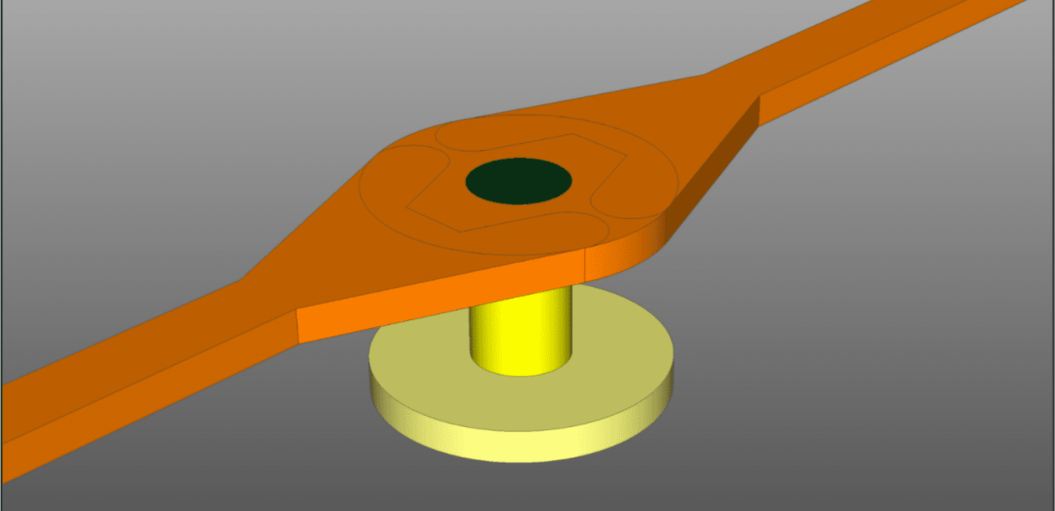
The addition of teardrops makes connections more durable and stable. They help to reduce mechanical stress and maintain the continuity of the circuit. Consider the difference between the via-to-track connections shown in Figure 1, and the same connections with added teardrops shown in Figure 2.
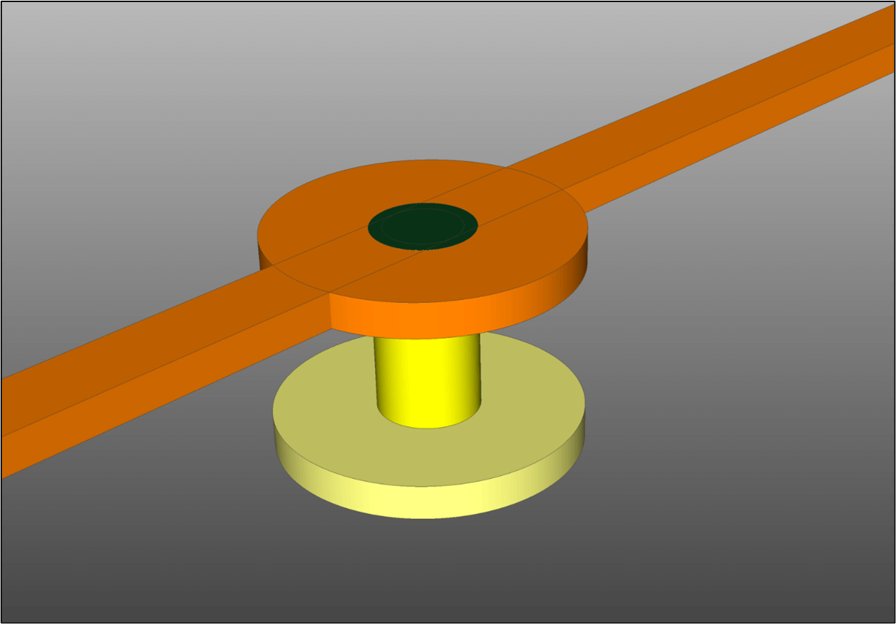
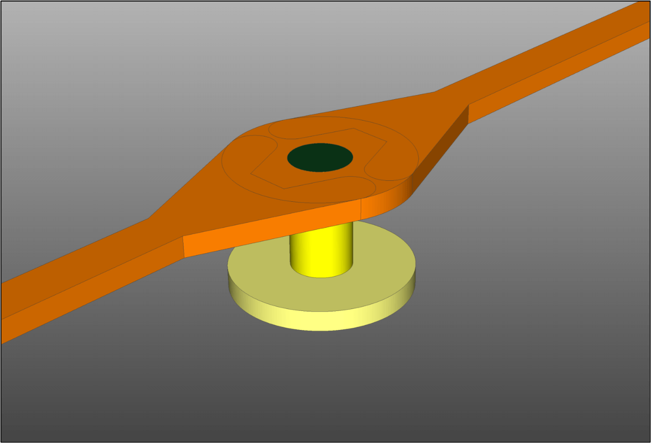
There are multiple benefits of using teardrops in situations like this.
Better durability and quality
There is a more gradual change of width, which reinforces the durability of the conductors in relation to environmental factors such as temperature, humidity, and mechanical stress.
Increased tolerance of manufacturing variations
The teardrops make the via more resilient regarding drill wander. The effective size of the annular ring is increased over much of its circumference. This could make the difference between success and failure for an entire PCB – increasing the yield of good boards in a production run.
Lower costs
PCBs that are more durable and more tolerant mean fewer failures and returns, and fewer hours spent in hardware debugging.
Check for design rule errors
Always consider design rules when adding teardrops because they can introduce subtle clearance errors. eCADSTAR can avoid creating DRC errors automatically.
PCB teardrops on track-to-track connections
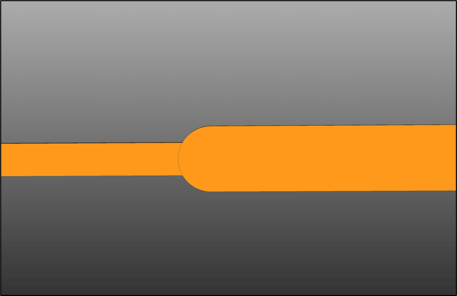
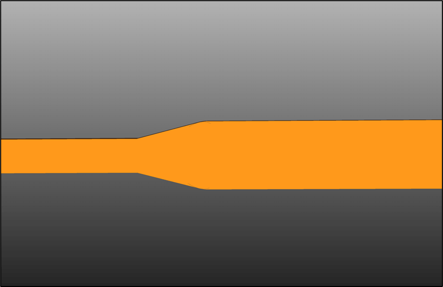
Teardrops on track-to-track connections yield similar mechanical advantages to teardrops on track-to-pad connections. They also bring more subtle benefits in high-frequency circuits because they create a more gradual electrical transition as well as a more gradual physical one.
In Figure 3, the rounded track ends still create a sharp junction, but when a teardrop is added as shown in Figure 4, the width change is more gradual.
In routing for high-speed circuits, the characteristic impedance is a key design parameter. Track width affects characteristic impedance and changes in characteristic impedance cause undesirable signal reflections at junctions. Teardrops mitigate that effect by making changes more gradual. In RF circuits such as on-PCB antennas, special track-to-track junction shapes are often specified in application notes. Depending on requirements, a teardrop can sometimes be added as an alternative to creating a custom conductor area.
Adding teardrops in eCADSTAR
Once teardrop styles have been defined, they can be set as part of the routing style and added automatically, and any DRC issues that teardrops might cause can be avoided automatically. Teardrops can, of course, be added manually too.
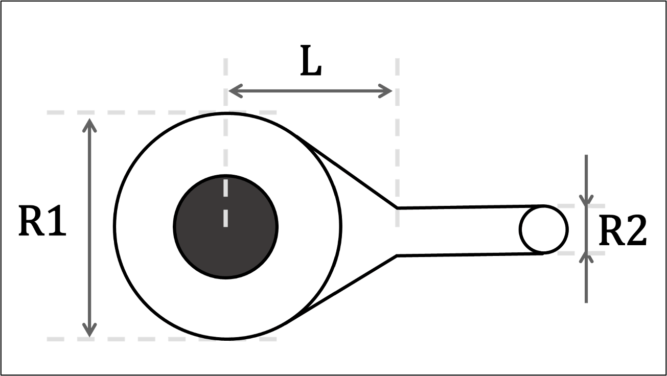
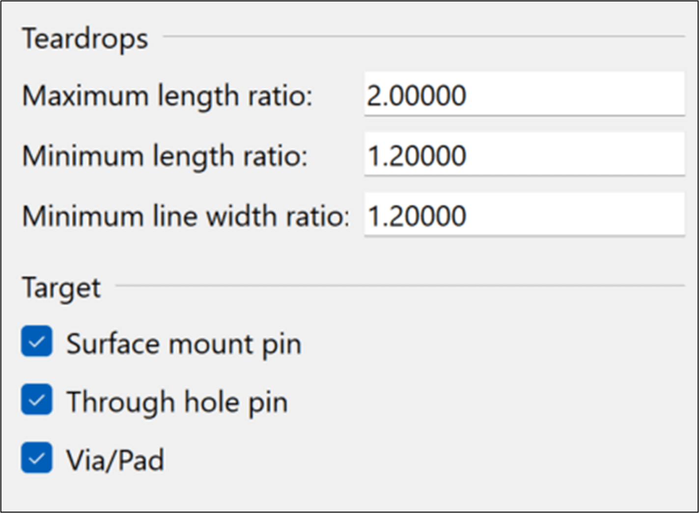
When you set up teardrop styles in eCADSTAR, it considers maximum and minimum length ratio. In the diagram shown in Figure 5, this ratio is L/(0.5(R1)) .
If the length ratio is set 1.0, then there is no teardrop.
The maximum length ratio defines the value of this ratio at the maximum extent of the teardrop.
Defining teardrop styles using ratios rather than absolute values means they can be used on multiple pad sizes and types.
The minimum line width ratio defines the minimum ratio between the widest and narrowest parts of the teardrop. In Figure 5, this ratio is R1/R2 , so the minimum setting for this ratio is 1.0.
Conclusion about PCB Teardrops
Teardrops are especially useful in both high-density PCBs and those that need high reliability in demanding environments, such as IPC Class 3. Teardrops are also mentioned, but not mandated, in IPC-221A.
Teardrops are needed more when track and pad geometries are smaller. They make circuit boards more environmentally resilient and more tolerant of slight manufacturing variations. If used correctly, they can help with thermal performance and optimising high-speed signaling too.
They are a valuable tool in what might be called “defensive design”: reducing the chance of problems at the margins.
If you are keen to learn more about PCB teardrops you can watch this video about how to add teardrops to improve your PCB designs

-
Jane Berrie•Signal Integrity Expert, Zuken Tech Center, BristolJane Berrie has been involved in EDA for PCB signal integrity since the 1980s. Her articles have appeared in many publications worldwide - too many times to mention. Jane is also a past session chair for 3D IC design at the annual Design Automation Conference. Jane’s also an innovator with a unique perspective, who constantly works on new solutions in the fast-evolving world of electronic design. In her spare time, Jane has organized themed charity events - including two in aid of lifeboats and red squirrel survival. Jane is also a regular disco-goer.
