
Reinforcing Vias
Reinforcing vias or stitching vias, connect conductor areas on different PCB layers together in definable patterns.
Menu
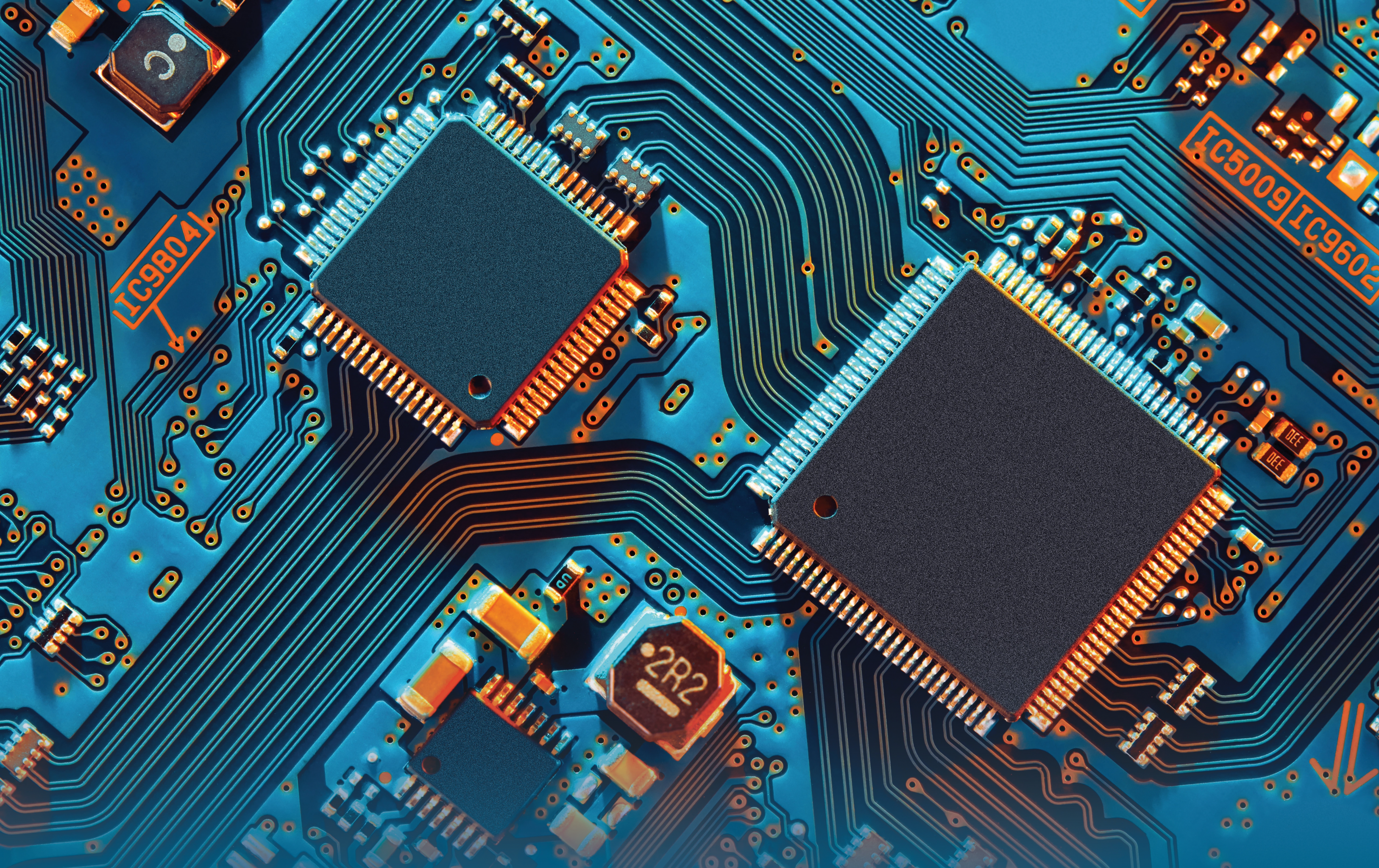
What are Reinforcing Vias?
Otherwise known as “stitching vias”, reinforcing vias connect conductor areas on different PCB layers together in definable patterns.
Benefits of Stitching Areas Together with Reinforcing Vias
- You can stitch conductor areas that require a low impedance between layers much more quickly and predictably
- It makes it easier to avoid errors such as overlapping via clearance gaps that create plane discontinuities
- You can be more reassured you have followed application-note rules for items like shield stitching
- It makes it easier to edit your PCB design to, for instance, change the vias types used for stitching
These three (1 minute) videos explain the basics of reinforcing vias in eCADSTAR
- The Science of Reinforcing Vias describes what reinforcing vias do in electrical terms
- Use Reinforcing Vias to Nail Down Power and Ground Areas presents an example of how you could use reinforcing vias in a popular kind of circuit— a buck (DC-to-DC step-down) converter
- Easy and Consistent Reinforcing Via Selection drills down to some practicalities of how to get the most from reinforcing vias in eCADSTAR

-
Jane Berrie•Electronic Design Technology PartnerJane Berrie is an EDA product innovator and technical marketing content creator, focusing on high-speed design and signal integrity. She is a published author of technical articles and a past session chair at the annual Design Automation Conference (DAC).
Ready to brush up on something new? We’ve got more videos to watch right this way.

- Press
May 06, 2026
eCADSTAR 2026.0 Release
Click Here!
Read now
New release enables faster design processes, easier data management, and improved handling of complex PCB projects.
- Products
February 19, 2026
What's New in eCADSTAR 2026.0
Key highlights of the eCADSTAR 2026.0 update
Read now
The 2026.0 release optimizes your workflow from design to library management, allowing for faster and more efficient execution.

- Press
November 11, 2025
Zuken-TME Partnership
TME brings real-time access to component availability, pricing, and ready-to-use EDA models directly into the eCADSTAR environment.
Read now
TME is expanding integrated services within Zuken’s eCADSTAR platform.