Stitching Vias to Lower PCB Power Impedance
Introduction to Stitching Vias
If you are reading this, you probably know what a PCB via is. It’s usually a plated hole that connects conductors on two or more PCB layers together – a connection made in the third dimension. Stitching vias are inserted in patterns, like stitches made by a sewing machine. Sometimes those patterns are regular and sometimes they are intentionally irregular.
I have seen many issues caused by insufficient attention to power impedance. They are easy to miss because these issues can be very subtle.
It’s easy to forget that the sudden power demands of fast-changing signals have to be supplied as cleanly as possible. The faster the signals switch, the more AC impedance comes into play in addition to DC resistance. Keeping impedance low in these areas is essential to avoid instantaneous voltage drops or ground bounce.
Impedance comprises the combined effects of resistance, capacitance, and inductance. Stitching conductor areas together mostly reduces the resistance between areas connected to the same power signals.
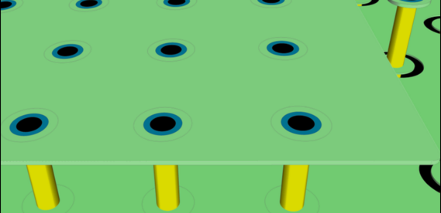
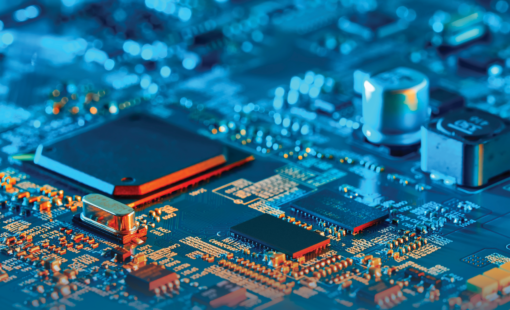
The stitching shown in Figure 1, between Vcc areas on two layers, is effective because the vias act mainly as parallel, low-value resistors.
PCB design applications like eCADSTAR let you set specific stitching via patterns and change them easily, and sometimes that’s essential because stitching vias work as a team.
So far I’ve mentioned stitching areas that carry the same power or ground signal together. But what about the impedance between power and ground areas? Clearly, you can’t solve that by stitching them together, because that’s called a short-circuit.
The impedance between plane areas that matters most for good electromagnetic compatibility is mainly related to capacitance. That’s why we add decoupling and bulk power supply capacitors. But the planes themselves also act as capacitor plates, which is one reason why primary power and ground planes are often on adjacent layers at the layer stack core.
Figure 2 shows the basic formula for the capacitance of a plate capacitor:
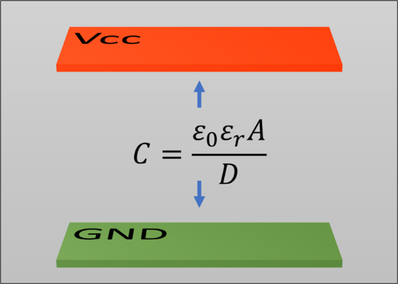
ε0 is a constant. εr is relative permittivity – in this case it’s the dielectric constant of the insulating material between power and ground in the layer stack. A is cross-sectional area.
The idea that these areas behave in such a cut-and-dried way is a gross simplification, but it provides a handle on what’s needed. Current and voltage change very quickly, and travel as waves, so there are many local effects on impedance, even within short distances in the same area.
Complications of Stitching Vias
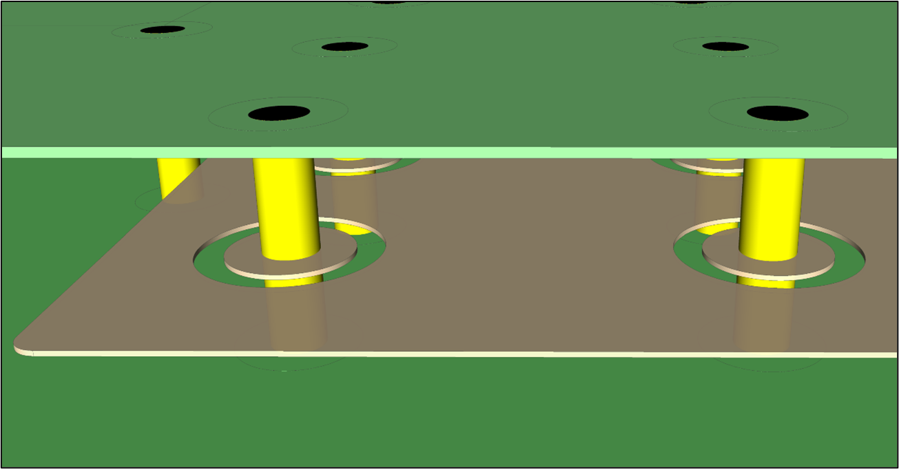
When you insert a stitching via pattern, you make holes in any area you don’t connect to.
If, for example, there’s a ground area between the stitched Vcc planes in Figure 1, then the stitching will puncture it (Figure 3). Those holes will increase DC resistance, because there’s more space and less metal, but in other ways, the holes can be a good thing, because they add capacitance between Vcc and Ground, lowering the overall power bus impedance.
This is not the only complication. Electromagnetic waves are subject to many AC effects. Irregular via patterns are sometimes used to avoid creating metal or void areas that tune to dominant frequencies. Those are not always simply clock frequencies. They can be harmonics (multiples of it) or even different frequencies entirely, related to the signal rise and fall times.
Other Uses of Stitching Vias
Stitching vias create conduction in the Z-dimension, and they introduce conducting cylinders that pass through insulating layers. This means they are useful in many other ways. The defining characteristics of stitching vias compared to vias, in general, is that they are laid down and edited in patterns.
Rows of grounded stitching vias can create a “fence” that reduces Electromagnetic Interference (EMI) and reduces the danger of external noise affecting circuits within the “fenced” area.
Vias are often stitched at regular intervals along grounded tracks or conductor shapes surrounding sensitive signals so that shields are electrically “nailed” to a ground plane.
The metal in via plating and pads also creates thermal conduction, so a pattern of stitching vias can carry heat away from sensitive components to ground or power planes elsewhere in the layer stack, by creating thermal via arrays.
Summary
The number one requirement is to keep power bus impedance low, in terms of both AC and DC. Stitching vias help a lot. They are definable patterns of vias that work in groups and can be added and edited as groups too. When a signal integrity engineer notices, say, that a different stitching pattern is needed, it’s quick and easy to make the change.

-
Jane Berrie•Signal Integrity Expert, Zuken Tech Center, Bristol.Jane Berrie has been involved in EDA for PCB signal integrity since the 1980s. Her articles have appeared in many publications worldwide - too many times to mention. Jane is also a past session chair for 3D IC design at the annual Design Automation Conference. Jane’s also an innovator with a unique perspective, who constantly works on new solutions in the fast-evolving world of electronic design. In her spare time, Jane has organized themed charity events - including two in aid of lifeboats and red squirrel survival. Jane is also a regular disco-goer.
- Blog

- Blog

- Blog
Discover how Quadra Solutions won the prestigious award and what it takes it win!
- Blog
Read more!