Designing Half-Plated Holes for SMD Modules
How to Design Half-Plated Holes for an SMD Module
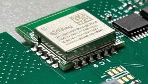
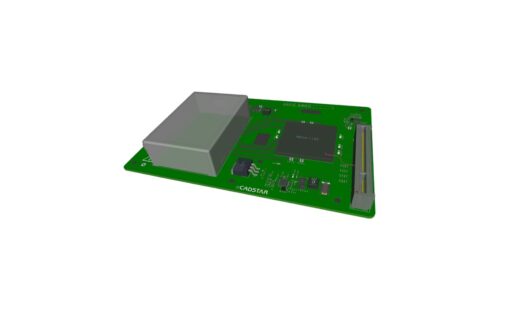
SMD modules like the DA14531MOD from Dialog Semiconductors (A Renesas 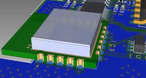 company) is a Bluetooth® Low Energy module using a particular plated hole style called half-plated (also called castellated holes). If you look at these modules, it should be evident how half-plated holes on a PCB can be used to mount a PCB module as an SMD component. These small modules are becoming more popular due to the global shortage of electronic components in the market. They are actually simple to work with, although they might look a bit specialized for use in the standard PCB fabrication process.
How to find electronic components when there is a shortage in the market
The first challenge is to find electronic components or alternatives when there is a shortage in the market. With eCADSTAR direct and online integration to some of the most of the world’s largest part vendors, viewing live part information including stock, pricing and alternatives is a breeze.
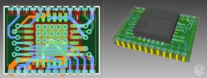
But often if the preferred part is not available, you end up with alternatives that do not match the already used footprint. Instead of redesigning and manufacturing a new version of the master board, you can just design a small interface board on which you mount a smaller alternative part and the total PCB module can be mounted as an SMD component. This allows you to mate a small module to your main PCB with SMD soldering. Half-plated holes are used on small modules as an alternative to pin-header mounting. Instead of using pin headers to mate two boards, you can design the main board with SMD pads to mount an array of half-plated holes.
Using half-plated holes on your module will provide a strong soldered connection between the module and your carrier board. To make this work, you need to design a half-plated hole array along the edge of your SMD module and ensure this will fit on the footprint of the part on your carrier board to hold your SMD module.
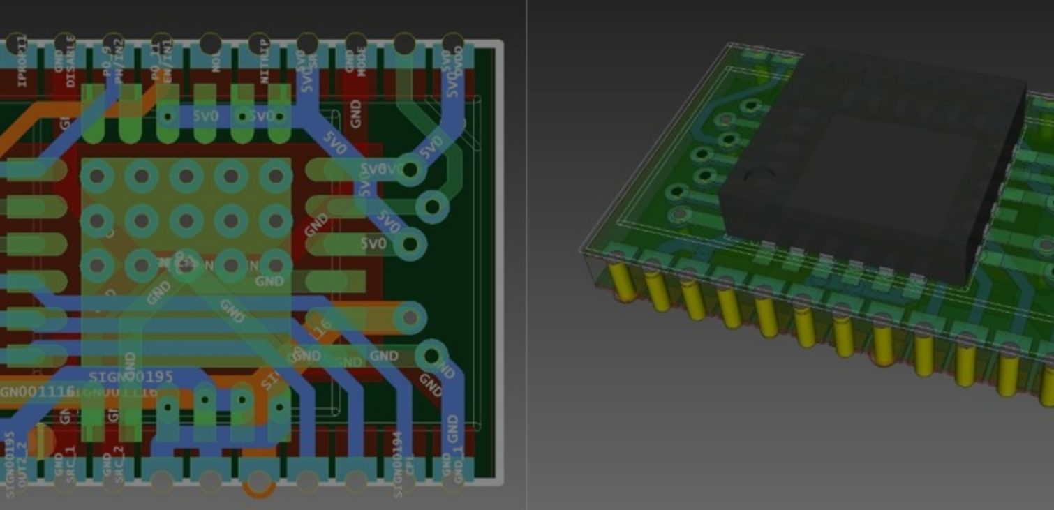
Example of a half-plated hole design in eCADSTAR for a motor driver module, using the DRV8256E (24-Pin VQFN with Exposed Thermal PAD footprint) as an alternative for the DRV8873H-Q1 (24 HTSSOP PowerPAD™ IC).
You’ll have to approach this while thinking about the fabrication process, but the basic tools in eCADSTAR can be used to easily place half-plated holes on your PCB.
The image above shows an example of how half-plated holes can be placed in eCADSTAR. Note that I’ve placed standard pads with plated through-holes, and the through-holes hang over the edge of the board. This overhang can be addressed in manufacturing.
Designing the Pad Array on Your Main Board
The pad array on the main board follows standard land pattern design guidelines for SMD components. Although the half-plated holes will be treated as a through-hole feature in the manufacturing process, to mount the module to your main board, it can be soldered just like other SMD components.
Some attention must be paid during assembly and soldering. A problem can be the potential for contamination; the pad array on the carrier board can trap exhaust from some fluxes during reflow soldering or too much solder paste along the pad array can lift the module. However, this is similar to what can happen with SMD ICs that have a large ground path in the center of the component. I have not experienced it as a problem, but if it occurs, you can overcome this by hand soldering or selective soldering. In which case you won’t have the potential for component liftoff or contamination from some fluxes during soldering.
In eCADSTAR, you can easily place half-plated holes in your PCB layout. You can also instantly create the fabrication files your manufacturer needs to correctly place your half-plated hole array.

-
Jeroen Leinders•eCADSTAR Business Manager Europe at ZukenJeroen Leinders has over 30 years of experience in various parts of the electronic industry in design, manufacturing, and EDA software. He is eCADSTAR Business Manager in Europe for Zuken, based out of his home office in the Netherlands. Where possible, exploring and developing new strategies, business opportunities, and areas for eCADSTAR. He is fascinated with the latest technical gadgets and enjoys riding his motorbike.

- Blog

- Blog

- Blog
Discover how Quadra Solutions won the prestigious award and what it takes it win!
- Blog
Read more!