2D 3D simultaneous pcb design for pcb designers hero image

What's New in eCADSTAR 2022

Here are just a few of the new features. If you’d like to learn more, contact your local sales representative.
Menu

2022 has been a strong year for eCADSTAR. We look forward to introducing exciting updates that will enhance your design experience.  The Schematic, PCB, and Library Editors have all been upgraded to address design needs you have told us are key for you.

Multi-Instance Hierarchy Design

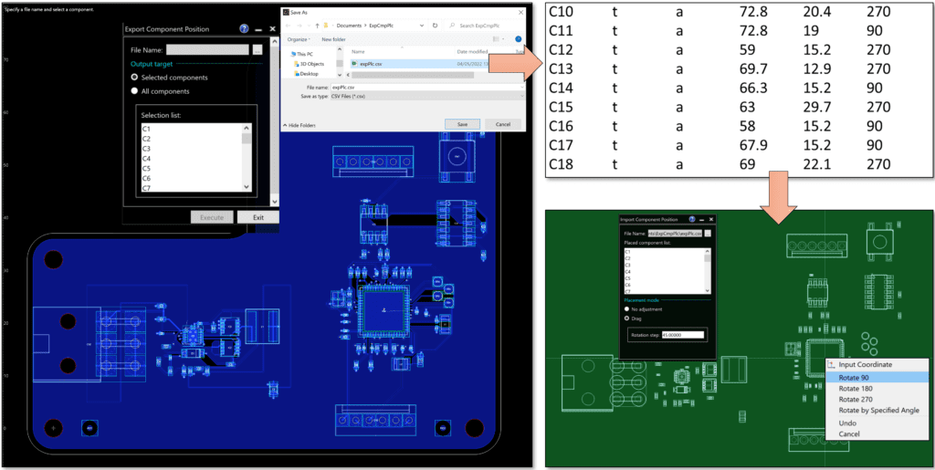
Structure schematics to maximize re-use opportunities and minimize copy/paste errors

  • Organize your schematics for clear interpretation and review
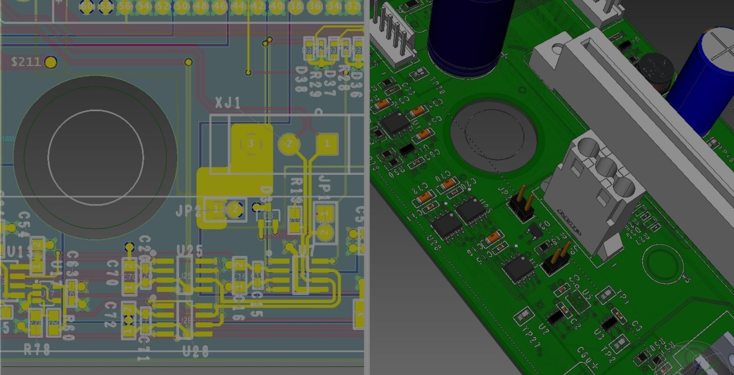
    • Block structure provides clear functional overviews and declutters reviews of special circuits such as RF
  • Avoid copy/paste in channeled or repeated sections of circuitry such as stereo amplifier channels or multiple USB I/O circuits
    • Define one block and create as many instances as you need
  • Instantly propagate block enhancements to all their instances
    • Upgrade key schematic circuits quickly and safely

3D Model Manager

Organize your 3D models to suit your standards, with crystal-clear 3D visibility

  • Rename, assign or delete 3D component models
    • Change model names to make it clear what each 3D model represents in your library – for example to match a corporate footprint naming convention
  • Organize models into subfolders or reorganize the ones you have
    • Bring structure and clarity to 3D component models, for example, organizing them according to package style
  • Import models from a wide range of popular 3D formats
    • Expand your choice of 3D model sources
  • Visualize models in 3D as you manage them
    • The model you have selected is the one you see, regardless of its name

Multi-Gate Reference Designator and FITTED/NOT FITTED Updates

Changes made to gated components automatically propagate to all affected symbols on all sheets in your schematic

  • Automatically propagate reference designator changes
    • Should you have one symbol each for four of a component’s I/O banks on your schematic, and you change the reference designator on one of them from IC7 to IC8, that change is automatically made on all four
  • Automatically propagate fitted/not fitted settings in design variants
    • If you change one NAND gate in a component containing four of them from NOT FITTED to FITTED, then the status propagates to any symbols on your schematic that represent the other three

Automatic Push-aside When Moving Components

Make small adjustments with less work

  • When you move a component, others are pushed aside to avoid spacing errors and tracks are re-routed in real-time
    • Best for small adjustments such as moving a component onto a coarser grid setting
    • You can set a pin count threshold to avoid disturbing large-pinout components
  • Preview what you will get and try different moves before committing one to your design

Clear Etch Factor Modeling and Dimensioning in Redesigned Configuration Editor

Etch factor changes parameters like characteristic impedance and propagation velocity, especially on closely-coupled differential pairs

  • Define the default etch factor in application settings, or set it for individual track configurations
    • Etch factor has a significant effect on coupling between parallel tracks
  • Etch factors can be saved with scenarios and retained in simulation
    • Improved accuracy for impedance and coupling
  • New user interface with many new features
    • Detailed dimensioning makes it easier to verify correctness of track configurations

Etch-factor-configuration-editor-1024x987

Clear-Etch-1-1024x579

Local Pin Type Editing for PI/EMI Analysis

Library-Pin-Types-799x1024

No library change is needed if library pin types are imprecise

  • Library parts often have pin types set to general-purpose values, for example, pins set as bidirectional are often used as inputs or outputs
    • Edit pin types directly in PI/EMI
    • Set all pin types correctly for optimum Power Integrity Analysis

Bidirectional Cross-probe Between PCB and Electrical Editors

Easily relate routing to high-speed transmission-line equivalent circuit

  • Verify electrical topology
    • Transmission lines cross-referenced to corresponding physical tracks
  • Optimize signaling performance
    • Explore alternative topologies with enhanced clarity


Multi-pad Footprint Pins Supported in all Routing Operations

Multi-pad-footprint-pins

A multiple-pad pin comprises multiple figures

  • Route to any pad that corresponds to a pin on a signal in the same way
    • Full routing support means easier, more efficient routing with less chance of error

Export and Import Component Positions

Reproduce known-good placement in multiple PCB designs

  • Reproduce component placement in other designs as well as within the same PCB
    • Export or import positions of selected components in .csv format


export-import-1024x515

To learn more about the many additional new features included in eCADSTAR 2022.0, get in contact with your local representative below!

Got a Question?

For more information on how eCADSTAR can optimize your design process, contact us today.
Contact Us