
High-Speed PCB Design and Copper Surface Roughness
Introduction to High-Speed PCB Design and Copper Surface Roughness
Planning proper signal transmission for today’s ultra-high-speed digital systems is getting more difficult due to the ongoing IC buffer-technology evolution and the consequently more complicated design requirements/constraints by diverse sources. Signalling standards (e.g., fast differential data transmission, SERDES links) and the implemented protocols (USB, SATA, PCIe etc.) cause increasing headaches for PCB designers. The lossy behaviour of the conductor material will degrade the performance of the signal transmission at higher data rates.
Taking a detailed look on how the surfaces of PCB traces look like in reality reveals yet another pain. In the PCB manufacturing world, things like perfectly smooth copper surfaces do not exist at all. There is always a certain degree of material roughness (which is fortunately beneficial for the adhesion of the copper to the dielectric material during the stacking of the different layers of a PCB). For high-speed digital designs in particular, the conductor surface roughness effect, which refers to the influence of the roughness of the conductor surface, influences the current flow across the geometry of signal traces.
With direct current (DC) and low-frequency alternating current (AC) situations, it does not matter that much, how rough the copper surface profile of a trace is. But in today’s high-speed applications in the GHz range (in terms of data rates), the conductors’ effective skin depth, defining where most of the current flow will take place, narrows very close to the root-mean-square height of the rough conductor surface. Surface roughness will then impact the current flow and cause a higher than usual loss. If you like, you can compare this situation with a race car that cannot drive as fast on dirty uneven farm roads compared with a flat racetrack.
To address this effect, most copper foil manufacturers offer specially made ‘smooth’ copper sheets, called electro-deposit (ED) foils, to be used on request in PCB manufacturing with varying degrees of roughness, directly impacting the production costs. Knowing the design margins is therefore a key factor in the success of the overall product design. And surface roughness certainly narrows down this margin.
Transmission Line Loss, Modelling, Attenuation, Skin Effect
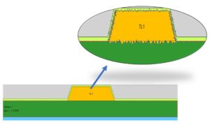
In recent years transmission lines are treated as lossy elements in the signal integrity (SI) analysis. The losses originate from various individual loss effects, like conductor loss, dielectric loss and to a lower extent radiation loss. All these various loss effects are frequency-, material-, and geometry dependent. At high frequencies (e.g., beyond 1 GHz), the effect of the surface roughness of the copper will impact the overall loss significantly. The better known “skin-effect” describes the tendency of currents to concentrate at the outer surface area of the conductor. This is illustrated in the picture below where the orange colour areas depict the different skin-depth on a copper trace cross-section.
The region between the outer surface and the point where the current density drops to about 37% of its value at the surface is called the skin depth. Calculating skin depth requires the frequency of the AC signal, the resistivity and relative permeability of the conductive material. It can be derived by the formula (1) below:
In this case, the skin depth δ (in m) is defined by the frequency of interest f (in Hz), µ is the permeability of the material (µo, or 1.2566E-6 H/m for most materials), s is the conductivity of the material (in Siemens/m or 1/r where r is the resistivity in ohm-m). Simplified (for the pure copper case), this can be reduced to the formula (2) below, which is good for a first order estimation (found in [9]):
δ=66* √(1/f) (2)
Just to show you that factor in its extremes: At 50 Hz In copper, the skin-depth is roughly about 9.3mm. At higher frequencies, the skin-depth becomes much smaller, down to 2µm at 1GHz (we do have this frequency in today’s communication links) and at a frequency of 50GHz, the skin-depth can be as tiny as a little less than 300nm (0.295µm).
The Impact of the Skin Effect and High-Speed PCB Design
When this area where the currents’ concentrates will be rather rough than smooth, the effective conductor length extends as the current tends to follow along the contours (I have to say: The real electromagnetic behaviour is slightly more complicated, details can be found excellently described in [3]).
At high-speed frequencies and the data rates of today’s SERDES links like PCI-Express, USB3, HDMI etc., the resulting effective resistance will increase (by conductor loss and dielectric loss) which will compromise the signal transmission and hence the bit error rate (BER) to some extent. The simulator-internal transmission line model comprising various lumped elements (per unit length) is impacted in considering frequency and material dependent losses (which do affect the R’ and the G’ parameters and therefore slightly modify propagation delay by increasing attenuation and dispersion).
Copper Surface Roughness and Loss Modelling
As signal integrity analysis has matured, several modelling methods have been developed over the years to determine a correction factor for the copper surface roughness. One of the most popular methods is the Hammerstad-Jensen model [6], where the theoretical approach uses the work of Samuel Morgan [1], who defined this concept in 1949 by introducing a mathematical “correction” for the roughness.
This “Morgan correlation factor” Kr for the conductor surface roughness describes the relative roughness of a conductor surface as the ratio of a smooth surface vs. a rough surface. According to [2], this model has been correlated sufficiently well for microstrip geometries up to multiple GHz and for a surface roughness of less than 2 𝜇m. However, it should be mentioned, that in recent years other models (like the Huray model [6]) have gained significant popularity for modelling high data rate interconnects.
Consideration of Conductor Surface Roughness in eCADSTAR Signal Integrity Analysis
Most electrical engineers concerned with all the different phases of their design project may not expect that they must deal with such copper roughness issues during their work – they assume, this involves just the technology people who do define the cornerstones of the board stack-up, the used materials and the details of the manufacturing process, and very likely, this assumption is correct in most cases. But another perception is not true: That such analysis requires the use of highly sophisticated 3D-EM simulation tools.
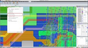
Correctly, it must be said, that 3D-EM tools are one way to address such questions and such tools are in fact very powerful to investigate all different aspects of current-flow, loss, conductor-roughness and skin-depth. And it is somewhat little known, that the embedded signal integrity simulation tools within eCADSTAR have implemented the Hammerstad-Jensen approach recently so that the user can force the simulator to include the roughness adjustment factor into the time domain and frequency domain signal integrity analysis. As shown in Figure 4, this can be enabled in the simulator options dialog, so no complicated settings and there is no performance degrade involved at all for the simulation processes.
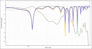
The impact becomes visible at higher frequencies/high data rates in both, time-domain simulation and frequency domain analysis. Examination of the simulated S-Parameters immediately shows the increasing impact vs. frequency. In Figure 5, the result of a FD simulation of a DDR4 signal is shown without and without the option set – at higher frequencies (the figure depicts the range between 500MHz and 10GHz), the relevant parameters (e.g., insertion loss) do show a rather small difference. But this may impact eye openings and the bit error rate estimations in SERDES simulations significantly.
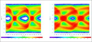
In Figure 5, the results of such a SERDES simulation (8GB/s) are shown with and without the surface roughness feature enabled, yielding significant different eye-opening characteristics.
Conclusion
In PCB construction things such as perfectly smooth conductor surfaces do not exist. I have never been an advocate to control impedance to two decimal places, but PCB designers must be aware that the skin-effect will have an impact on the AC resistance of high-speed signals and therefore the signal shapes beyond certain frequencies will be affected – with a chance to close the eye pattern. These days, practical methods for modelling conductor surface roughness have been widely established, one of those is implemented for as easy as possible use in the eCADSTAR Signal Integrity simulation suite.
These days with data rates exceeding multiples of GHz in a wide range of applications, knowing the basic concepts of transmission line behaviour is paramount. eCADSTAR allows you to conduct all the relevant analysis steps as an integral part of the design process without the need for complicated 3d party tools. In the end, I’d like to quote the great Eric Bogatin, just in case, you ask yourself, whether you have to take care of conductor surface roughness and its impact on the skin-effect: ‘It depends …’. But for sure, the results of integrated signal integrity analysis just one mouse-click away from your layout tool may help you to prevent scrap on the PCB manufacturing floor.
References:
1) Samuel P. Morgan, “Effect of surface roughness on eddy current losses at microwave frequencies,” Journal of Applied Physics, vol. 20, no. 4, pp. 352–362, Apr 1949.
2) Bert Simonovich: “Practical Method for Modelling Conductor Surface Roughness Using Close Packing of Equal Spheres”, 3) DesignCon 2015
3) Eric Bogatin, Yuriy Shlepnev, Chun-Ting “Tim” Wang Lee: “Back to basics: the onset of skin effect in circuit board traces”, DesignCon 2017
4) Yuriy Shlepnev, Chudy Nwachukwu: “Practical methodology for analysing the effect of conductor roughness on signal losses and dispersion in interconnects”, DesignCon 2012
5) Hinaga, Koledintseva, Anmula, Drewniak: “Effect of Conductor Surface Roughness upon Measured Loss and Extracted Values of PCB Laminate Material Dissipation Factor”, IPC 2009
6) Erick Bracken; “A Causal Huray Model for Surface Roughness”, DesignCon 2012
7) E. Hammerstad and O. Jensen, “Accurate Models for Microstrip Computer-Aided Design,” in IEEE MTT-S Intl. Microwave Symposium Digest, Washington, DC, 1980.
8) Eric Bogatin et al.: “Which one is better? Comparing Options to Describe Frequency Dependent Losses”, DesignCon 2013
9) Ness Engineering: Skin Depth Calculator
10) Wikipedia: Skin Effect

-
Ralf Brüning•Product Manager/Senior ConsultantRalf Brüning is a product manager involved in the development and deployment of Zuken’s analysis and high-speed solutions for the past 20 years. Ralf works to improve customer design processes and solve complex technical challenges associated with high-speed signal transmission, power integrity problems, and EMI emissions. In his free time, Ralf likes to golf, cook for his family and listen to rock music.
- Blog

- Blog
- Blog
Discover how Quadra Solutions won the prestigious award and what it takes it win!
- Blog
Read more.