Introduction to Power Integrity in PCB Design
Definition and Significance
Power integrity in PCB (Printed Circuit Board) design is a critical aspect that is concerned with the capability of the circuit board to effectively distribute power to its various active components without incurring significant loss or distortion due to unwanted resonances. This concept is increasingly significant in modern electronics, as the miniaturisation of components and the increasing functionality have heightened the sensitivity of today’s integrated circuits to even the slightest fluctuations in power. The precision required in modern electronic devices means that power integrity is no longer just a desirable feature just further improving reliability and EMC compliance but a fundamental necessity deciding on the success or failure of a hardware project. Power integrity compliance ensures that every component receives the correct voltage levels and the necessary charge to operate correctly, which is vital in high-performance applications.
Crucial Nature of Maintaining Power Integrity
The importance of maintaining stable power integrity cannot be overstated. Together with the overall PCB stack-up design a stable and reliable power distribution builds the basement upon which the functionality and reliability of a PCB are constructed. Inadequate power integrity can manifest in various impairments. System instability is a common issue, where unpredictable behaviour of the critical active components (CPUs, FPGAs, DSPs) can compromise the usability and reliability of the system. Data corruption (wrongly latched data), can result from transient power glitches, leading to loss of information and system failures. In severe cases, not maintaining power integrity properly can lead to a complete failure of the PCB. Such often non-deterministic failures not only necessitate costly repairs or replacements but can also have broader implications in critical applications such as medical devices, aerospace, or telecommunications.
Thus, the quest for flawless power integrity is a cornerstone in today’s high-speed PCB design, demanding careful consideration to many details, extensive testing (virtual prototyping is strongly recommended here), and a deep understanding of the underlying effects and the impact of both, the components and the overall system architecture. As electronics continue to evolve, the challenge of maintaining power integrity becomes more complex, emphasising its critical role in the successful operation of modern electronic devices.
Challenges and Solutions in Power Integrity
Common Issues in PCB Design
Maintaining power integrity is fraught with various challenges. Among the most dominant ones are unwanted resonances and voltage drops, transient currents, and ground bounce, each capable of significantly impacting the performance and reliability of a circuit board.
Resonances: PCB power-plane Resonance occur when electrical energy oscillates between the magnetic field (inductive and capacitive effects) between power-ground plane pairs (which do form a plate capacitor). Resonant circuits can generate higher voltages or currents than are fed into them. Beyond impacting the power-delivery, resonances and anti-resonances can create very effective EMC antennas causing the board to radiate in the resonance frequency areas.
Voltage Drops: Voltage drops across a PCB can occur due to inadequate power delivery or excessive current draw from components. This issue is particularly pronounced in high-current applications, where the resistance of the traces and vias can lead to significant voltage differences in particular when many fast Ios do switch in parallel creating increased power demands.
Transient Currents: These are sudden bursts of current that can occur during the switching of digital circuits. Rapid changes in current levels can lead to voltage fluctuations, which in turn can disrupt the normal operation of sensitive components.
Ground Bounce: Ground bounce, or ground noise, is a phenomenon where the ground voltage level fluctuates due to inductance in the ground path. This can be particularly problematic in high-speed digital circuits, where the switching of numerous transistors can lead to significant variations in the ground potential impacting the switching levels (zero to one transition) and the noise margins
These issues often originate from a combination of causing factors, including inadequate decoupling, improper PDN layout, and unsuitable component or technology selection. Inadequate decoupling results in inadequate buffering of the power supply, leading to fluctuations in voltage. An improper PDN layout can worsen issues like electromagnetic interference (EMI) and signal crosstalk, while unsuitable component selection can lead to mismatches in power requirements and the delivery capabilities from the energy sources (VRMs) to the different load/sinks.
Strategies and Solutions
Tackling power integrity challenges requires a multifaceted approach, focusing on both, preventive measures in the design phase and corrective actions during the testing and analysis stages of the PCB layout, at best using integrated PI analysis tools to your benefit.
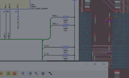
Proper Decoupling Techniques: Implementing effective decoupling involves placing capacitors following the IC vendor rules carefully and if possible close to power-consuming components. Match when possible (board real estate) the required number and allocation to the IC power pins. These capacitors then act as local energy reservoirs, supplying power during transient demands and smoothing out voltage fluctuations, therefore the chosen capacitance and the capacitor parasitics (ESL, ESR, capacitor package impact) play an important role too.
Adequate Power Plane Impedance: Maintaining a low impedance level in the power plane is crucial for minimising voltage drops and ensuring stable power delivery. This involves careful design of the power distribution network, considering all capacitive and especially inductive characteristics of the PDN elements.
Thoughtful Component Placement and Routing: The placement of components and the routing of power traces (if used, try to copper areas wherever possible, if power trace connections are needed make them wide and low-inductive) play a significant role in mitigating power integrity and EMI issues. Strategic placement of critical ICS (fast switching ICs with many power-pins and high energy demand) can help reduce the loop areas with their inductive effects that contribute to these problems.
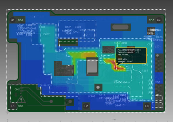
Use of Simulation Tools: Advanced simulation tools are essential in modern PCB design. They allow designers to analyse the power distribution network before the board is physically manufactured. These tools can identify potential issues such as plane resonances, voltage drops and transient currents. They enable designers to make pre-emptive adjustments. The simulation also aids in optimisation the layout for minimal noise and interference or to judge the decoupling scheme and in what-if studies helping to save non-necessary capacitors to save costs and board real-estate.
In summary, maintaining power integrity in PCB design is a complex task that requires careful consideration of various factors. Addressing challenges like decoupling and IR-Drop requires a holistic approach, a combination of well-thought-out design strategies, effective use of simulation tools, and rigorous testing. By taking these steps, designers can ensure that their PCBs deliver stable and reliable power, which is essential for the optimal performance of electronic devices.
Understanding the Power Distribution Network (PDN)
Role in Maintaining Power Integrity
The Power Distribution Network (PDN) is the cornerstone of the power integrity behaviour in PCB design, functioning as the primary conduit for distributing power across the entire circuit board. It plays the central role in ensuring that all components receive the necessary charge and the voltages reach the power levels to operate effectively and reliable. An optimised PDN is designed to minimise power losses and suppress parasitic noise, both aspects are crucial for the stable and efficient operation of the PCB.
Key Components of an Effective PDN
An effective PDN incorporates several elements, each serving a specific purpose in maintaining power integrity:
Capacitors for Decoupling: Decoupling capacitors are essential in stabilising the voltage supply and filtering out noise. They are strategically placed close to power-hungry components to provide a local energy reservoir for transient power demands.
Inductors for Filtering: Inductors are used in PDNs to filter out high-frequency noise. They act as a barrier against unwanted electromagnetic interference (EMI), ensuring that such disturbances do not propagate through the power network.
Well-Planned Layout: The physical layout of the PDN is crucial. This involves careful planning of trace widths, placements, and the distribution of power layers within the PCB. Proper layout helps in minimising resistive and inductive losses, ensuring efficient power delivery across the board.
Consideration of Trace Widths and Placements: The design of power traces plays a significant role in the effectiveness of the PDN. Wider traces can carry more current and reduce voltage drops, while the strategic placement of these traces can minimise inductive coupling and EMI.
In conclusion, the PDN is a vital element in PCB design, necessitating meticulous planning and execution. By understanding and implementing the key components and principles of an effective PDN, designers can significantly enhance the power integrity and overall performance of their PCB systems.
Correlation Between Power Integrity, Signal Integrity, and EMI
Impact on Signal Integrity and EMI
The relationship between power integrity, signal integrity, and electromagnetic interference (EMI) is a significant interdependency impacting the PCB design process. Power integrity has a direct impact on signal integrity. When power integrity is compromised, it often leads to fluctuations in the voltage levels and noise on the power supply rails. These fluctuations can induce signal distortions, malfunctions and false switching but as well jitter, which especially high-speed circuits interfaces (e.g.; PCIe, Ethernet) may harm an accurate data transmission.
Moreover, power integrity issues can increase electromagnetic interference (EMI) problems as the involved capacitances and inductance do create parasitic EMC antennas also, therefore inadequate power delivery and PDN noise can lead to the generation of unwanted electromagnetic fields, which then interfere with nearby electronic components and systems. EMI can propagate both through conducted and radiated paths, affecting not only the PCB itself but also other devices in its vicinity.
Mitigating EMI for Enhanced Power Integrity
Addressing EMI concerns is crucial for maintaining both, power and signal integrity. Shielding techniques are commonly employed to contain electromagnetic fields and prevent interference. This involves using shielded enclosures or layers within the PCB to protect sensitive components from external EMI sources.
Careful trace routing is another essential strategy. By strategically routing power and signal traces, designers can reduce the risk of crosstalk and electromagnetic coupling. This includes maintaining adequate spacing between traces, avoiding parallel routing of high-speed signals, and using ground planes effectively to shield signals.
Adherence to Electromagnetic Compatibility (EMC) standards is also vital. These standards are designed to ensure that electronic devices operate correctly in their intended environment without causing or suffering from EMI. Designers must be aware of and comply with these standards to ensure that their PCBs do not emit excessive EMI and are immune to external interference.
Finally, the use of differential signalling can be a powerful method to enhance signal integrity in the presence of EMI. Differential signals, which are transmitted using two complementary signal lines, are inherently more resistant to electromagnetic interference. This is because any interference tends to affect both lines equally and is cancelled out when the receiver calculates the difference between the two signals.
The interplay between power integrity, signal integrity, and EMI is a critical consideration in PCB design. By understanding these relationships and employing strategies such as shielding, careful trace routing, adherence to EMC standards, and differential signalling, designers can significantly improve the performance and reliability of their PCBs.