Signal Integrity and Why is it Important?
It is, perhaps, a truism to say that the electronics world never stands still. The relationship between the increasing performance of electronic equipment and demands for new applications is more complex than it first appears – are new applications possible thanks to the increased performance of chips, or do new applications drive the development of ever-higher performance electronic circuits?
However, it is indisputable that devices and the systems they enable continue to increase in performance at an incredible rate. One of the ways to increase performance is to drive the clock speed of your processor. This will decrease switching times and increase signal speeds and data rates overall. However, generally speaking, the faster a system is operating, the more a designer will be required to pay attention to signal integrity (SI) issues. This article aims to explain SI in general, consider its causes, and suggest PCB design approaches that will ensure SI.
In any system, electrical signals pass along different interconnections including the IC die to chip package connection, the package to PCB track, and connections between and through components, including connectors which can have also considerable internal signal paths. In simple electronics schematics, a connection is represented by a plain line. But in the real world, connections are metal wires or tracks that have resistance, capacitance, and inductance.
These result in parasitic elements – functions that are not desired for the operation of the circuit and which can have a detrimental effect on it. At low operating speeds, parasitic effects can often be ignored. However, at higher frequencies, capacitance and inductance may cause the wire to act as a transmission line, and antenna effects can cause EMI. Other issues such as crosstalk may also arise.
Almost everything in our electronic world has increased in frequency over the last few decades. Remember the old 4:3 standard definition TVs? That’s around 6MHz content. HD is almost a thing of the past with consumers now looking for 4k, and UHD products are being developed that increase speeds even further. The desire for more processing power has seen clock speeds increase steadily – from 16MHz of the 486 processor (which the hobbyist would overclock to increase performance) to today’s Ryzen ThreadRipper 3990X desktop PC CPU from AMD which features a 2.9 GHz base clock and a 4.3 GHz max boost clock.
This is all so we can process more information, more quickly – creating a better experience, with less ‘wait time’ for the consumer and higher perceived performance. Not all applications need the highest speeds, but many do which raises the game across the board. Whether it’s the speed of our internet downloads (no more waiting for images to slow-reveal themselves line by line) or the resolution of the camera on our phones, our world is undoubtedly getting faster. Even if a particular market segment doesn’t have its own pressure to increase speed, the components available are mostly increasing in speeds, and as such, it’s an issue we all have to deal with when it comes to designing PCBs.
What is SI and How Does it Impact Designs?
Signal integrity (SI) is the art of getting the signal you want from A to B, without any additional noise or interference – basically without being changed or compromised.
Anytime a signal is moved around, whether it’s along cables, across a PCB, or within a chip, SI needs to be considered. It’s not possible to maintain 100% integrity – when a signal is transmitted through a medium there will be losses. The goal is to reduce these losses and noise sources as much as possible and to maintain as good SI as possible.
There are many sources of signal degradation, and we will explore these. Let’s start with how the signals are moved around. This is increasingly important in high-frequency signals and brings up issues that were negligible at lower frequencies, so perhaps haven’t previously been an issue.
We have all experienced instances where cables cause visible interference on a screen, or audible noise is heard via an amplified system.
These are macro examples of how a cable can create SI issues for another piece of equipment. PCB designs are miniature versions of this, where a switching regulator can interfere with the DSP, or the ground noise from a CPU can travel through the ground plane and cause havoc with the analog signal processing. Whilst those are obvious examples, as speeds involved increase, we need to design the PCB with SI in mind.
Figure 1: Noise can travel through the ground plane causing interference with sensitive components
By understanding the sources of degradation, we can use good design practices to minimise and avoid SI problems. As the old saying goes, prevention is much better than cure; it is much easier to avoid the issue using good design practices than it is to clean it up afterward.
Fortunately, we do not have to break new ground here. RF designers have been dealing with high-speed SI issues for a very long time, and so there is a good body of information to draw on and adapt to new applications.
What Role Does PCB Layout Play in Signal Integrity?
Can PCB layout cause significant SI problems? Absolutely. Many SI problems are simply not present in a design until it takes a physical form. In the early design stage, a connection is represented by a simple line. The reality is a physical PCB trace with an impedance that is dependent on track size, spacing and shape, the board material, and parasitic effects created by the physicality of its surroundings.
This means that a circuit modeled in SPICE and appearing to be perfectly good, may not function once laid out. More often, the performance is degraded, much like the interference on a screen, and the end result is not acceptable. This can be costly if a whole production run has been fabricated, not to mention the knock-on effects of production delays.
Let’s take a look at the most common SI problems and best practices in PCB design
Design Considerations for Improving SI in PCB Traces
Impedance matching – a mismatch in impedance, whether it is between traces or from a trace to a connector, can cause serious problems. When the signal encounters a mismatch in impedance, only part of the signal moves forward, and the other portion of the signal is reflected back (a reflection). This creates two issues – firstly, the signal that is transmitted is reduced, making it more susceptible to noise – the signal-to-noise ratio (SNR) is reduced.
The second issue is the reflection traveling back down the trace is now noise. This reduces the signal integrity (SI) of the original signal and potentially creates further reflections. Last but not least, noisy signals are more likely candidates for crosstalk issues.
There is no single correct impedance – different standards use different impedance values; it’s matching the impedance that is important. A connector’s impedance value might be slightly mismatched – this can be compensated for in a good layout.
Transitions – High-speed signals should not be routed through multiple connectors or vias. Each of those connections/transitions can be a source of degradation of the signal, and also a chance for the signal to radiate and create interference elsewhere. Designing the high-speed signal paths first, to keep them short, rather than fitting them in around other routing, will help maintain good SI.
The shape of a trace – at RF, sharp bends in PCB traces can impact SI.
If possible, ensure sufficient space between tracks, not only for SI reasons but also for manufacturability.
How to manage noise sources for improved signal integrity
Sources of Noise – In the broadest sense, if it’s not your signal it’s all noise. Here are some key areas to consider in PCB design.
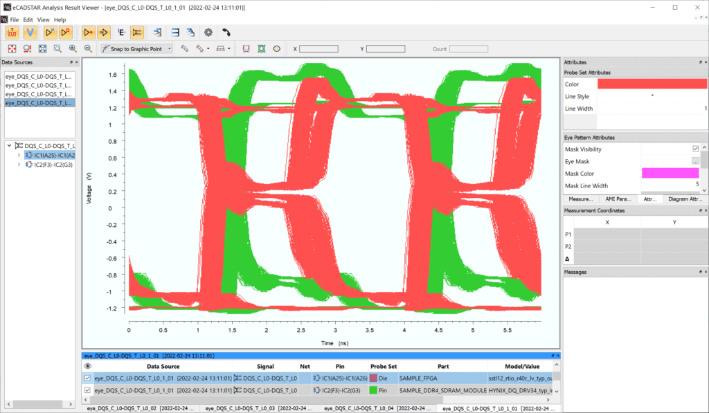
Differential pairs – this is a useful approach to protect signals from noise. The noise will be common on both lines, but the signal is the difference, and so the noise can be rejected at the end of the transmission, recovering the original signal. This technique has been used in cabling for a long time and is also popular in PCB traces. To maintain SI, the two traces of the differential pair must match exactly. The distance traveled and the impedance is key to the integrity of the signal but is not always an aspect that is handled well by automated tools.
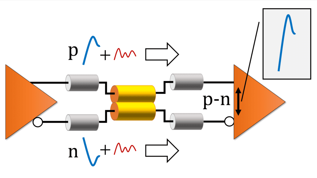
Figure 2: Differential pairs – help protect signals from noise
The unintentional antenna – The higher the frequency, the shorter the wavelength. An antenna is most effective when its physical length is ¼ of the wavelength of the signal. A radio/audio signal is a low frequency, hence a long wavelength, requiring a radio antenna to be fairly long. Mobile phones once had extendable antennas, but now they use PCB traces to create internal antennas.
As their frequency is high, the antennas only need to be short. This ably demonstrates how a PCB trace can become an antenna, and how, as speeds increase, even short PCB traces can become antennas. To minimise this, keep traces for high-speed signals as short as possible. Remove any extra traces or traces that extend past a connector, even in low-frequency areas. The old practice of laying down extra traces, in case some fixes were required, must be consigned to history.
Crosstalk – Some signals are inherently noisy (lots of fast transitions and switching); others are inherently sensitive (low amplitude, analog signals). Any two adjacent PCB traces will impact each other through induction. A change in one will cause a smaller, but similar change in the other. Therefore, noisy signals should be separated from sensitive signals either by distance – using specific areas or planes on the board – or by protecting them from each other using grounding shields and ground planes.
Multi-layer boards mean we need to consider crosstalk between layers. A simple rule is to route consecutive layers at right angles to each other. Using ground planes to isolate sensitive layers is also good practice for maintaining signal integrity.
Power supply noise is a major consideration and requires careful design. Switching regulators can introduce noise, linear regulators may still have ripple. A good practice is to have separate supplies for digital and analog sections. Check the switching frequency: is it in the middle of your signal bandwidth? Many switchers are programmable, enabling the noise to happen at a less intrusive frequency. Using a good filtering/decoupling network is essential.