PCB Technology & Design Rules
PCB technology and design rules are part of your master library. You manage them in Library Editor, just as you do with other library data, so there is just one short learning curve.
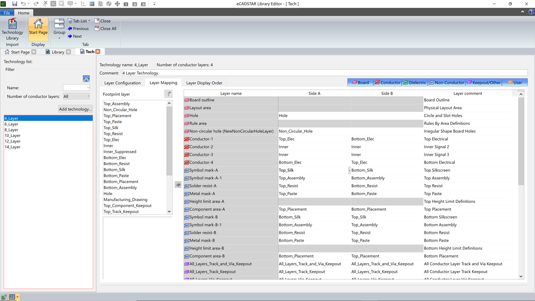
PCB technology and design rules are structured for maximum re-use. That does more than save valuable time—re-entered data is error-prone data.
With eCADSTAR, once data is entered and verified, it becomes premium IP that you can build on with confidence.
A layer stack need not be identical to re-use a PCB technology. If the top and bottom PCB layers, or a pair of inner layers are the same, then it’s much safer and more efficient to reference just one master definition. If a set of spacing or track width rules are the same on completely different layers, then the same applies—define once and then reference as many times as you like.
A layer stack need not be identical to re-use a PCB technology. If the top and bottom PCB layers, or a pair of inner layers are the same, then it’s much safer and more efficient to reference just one master definition. If a set of spacing or track width rules are the same on completely different layers, then the same applies—define once and then reference as many times as you like. 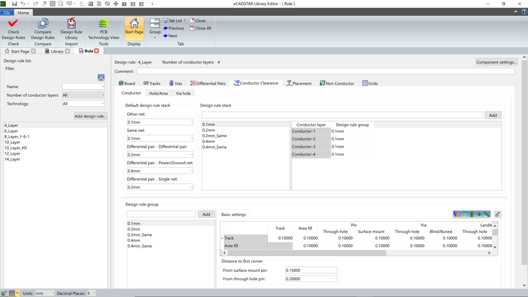
This philosophy carries over into the PCB design itself. If your PCB layout has a different number of layers from your reference layer stack, you can just pick the ones you want to create your production stack.
And if you need to, you can customize PCB technology and rules locally, in your design itself.
PCB technologies define materials, layer thicknesses, layer types, and layer stacks that you use to create PCBs. Design rules are settings like track widths, via spans, differential pair spacings, and clearances that you apply during PCB routing and placement. Technologies and design rules are structured for maximum re-use, including design rule stacks that you can compose from known-good lower-level rules.
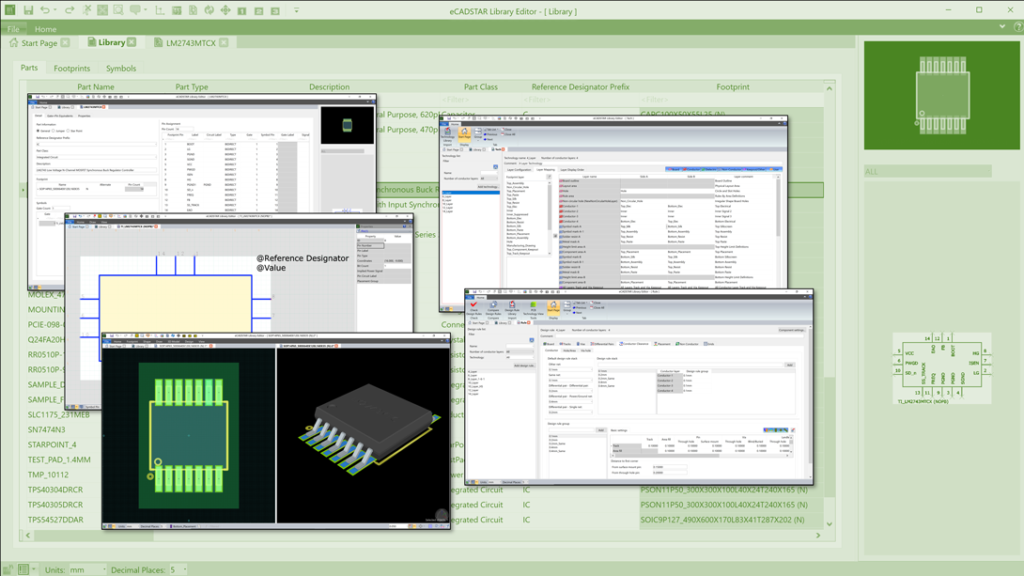
Schematic Symbols, Parts, PCB Footprints, Padstacks, Pads & 3D Models
With Library Editor, you manage all the key items you put on your schematics and PCBs in one place—even if you merge online parts into your library. A straightforward, consistent user interface. A true Windows GUI, so easy to use side-by-side with other applications. For example, adding data from one library to another is a straightforward copy and paste.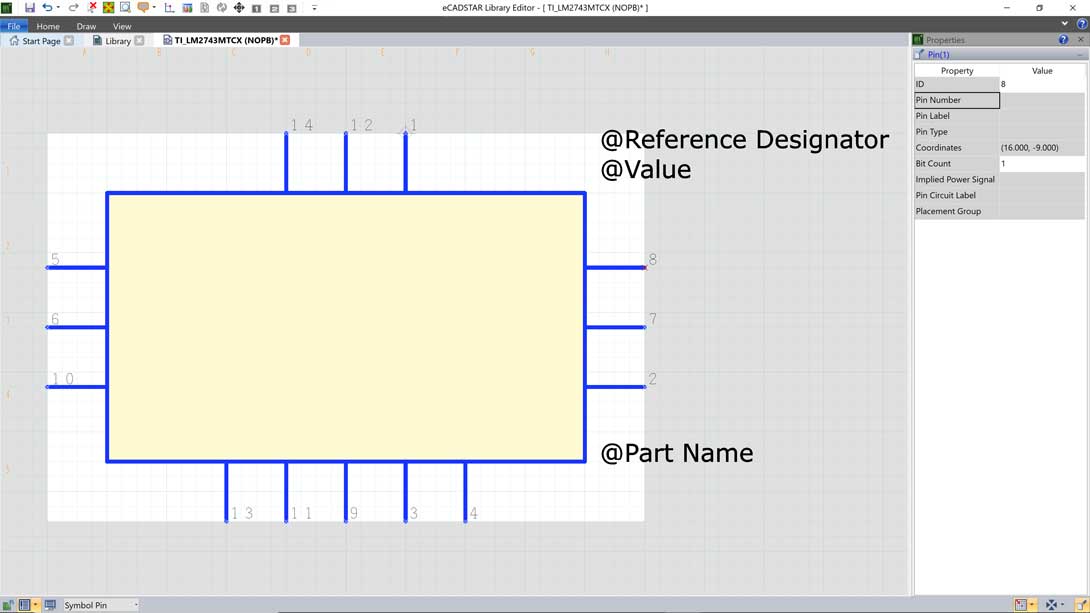
Schematic symbols often represent parts or functions within them, but they can also be items like sheet connectors, power supply voltages, and routing star points.
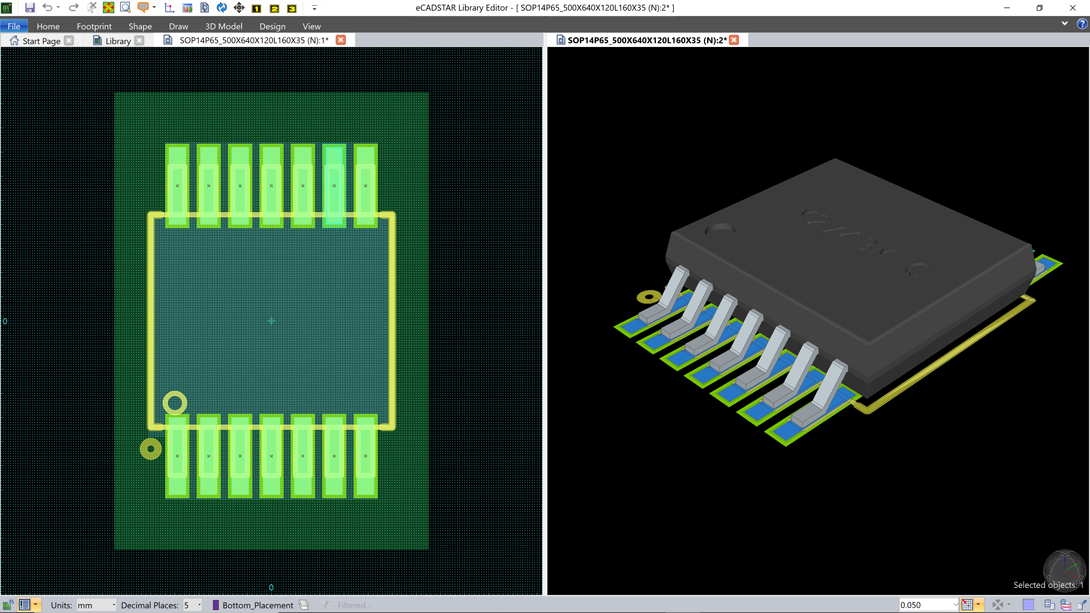
PCB footprints are what gets imprinted on the unpopulated PCB for a component. Pads, conductor shapes, solder mask, and any other data layers. You can include documentation layers too. PCB footprints can consist of 3D models. You can import STEP format models and these are often included in data for web parts.
Parts unite schematic symbols and PCB footprints, managing pin assignments and settings like legal pin swaps and the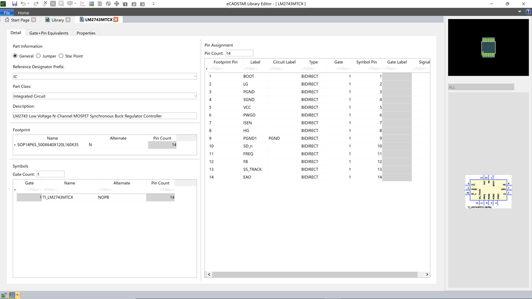 symbols used to represent each function (called “gates”, but can be items such as IO banks or multi-voltage power supply symbols).
Just as with PCB technology and design rules, these items are structured for maximum re-use and minimum repetition. You can independently create and edit pads, padstacks, PCB footprints, the parts that use them and the symbols that represent those parts—but without switching applications.
You can download web parts and merge them directly into your library. Once in the library they become fully editable and you can adjust them to, for example, comply with your company standards. eCADSTAR features direct integration to some of the world’s largest part vendors and online component libraries, including Allied Electronic & Automation, Arrow, Digi-Key, Transfer Multisort Elektronik (TME), Mouser Electronics, RS, SamacSys, SnapMagic and Ultra Librarian.
You can open schematic symbols, parts and PCB footprints for editing from Library Editor’s main tab. When you edit footprints, you can even split to multiple views in any mix of 2D and 3D, to avoid later surprises due to out-of-view errors. Built-in access to cloud component libraries, including electrical schematic symbols, datasheets and 3D models makes PCB prototyping fast and accurate and you can manage part obsolescence and sourcing dynamically. With eCADSTAR’s fully-structured PCB parts libraries, you only enter data once and re-use it anywhere, bringing greater efficiency, accuracy and reliability.
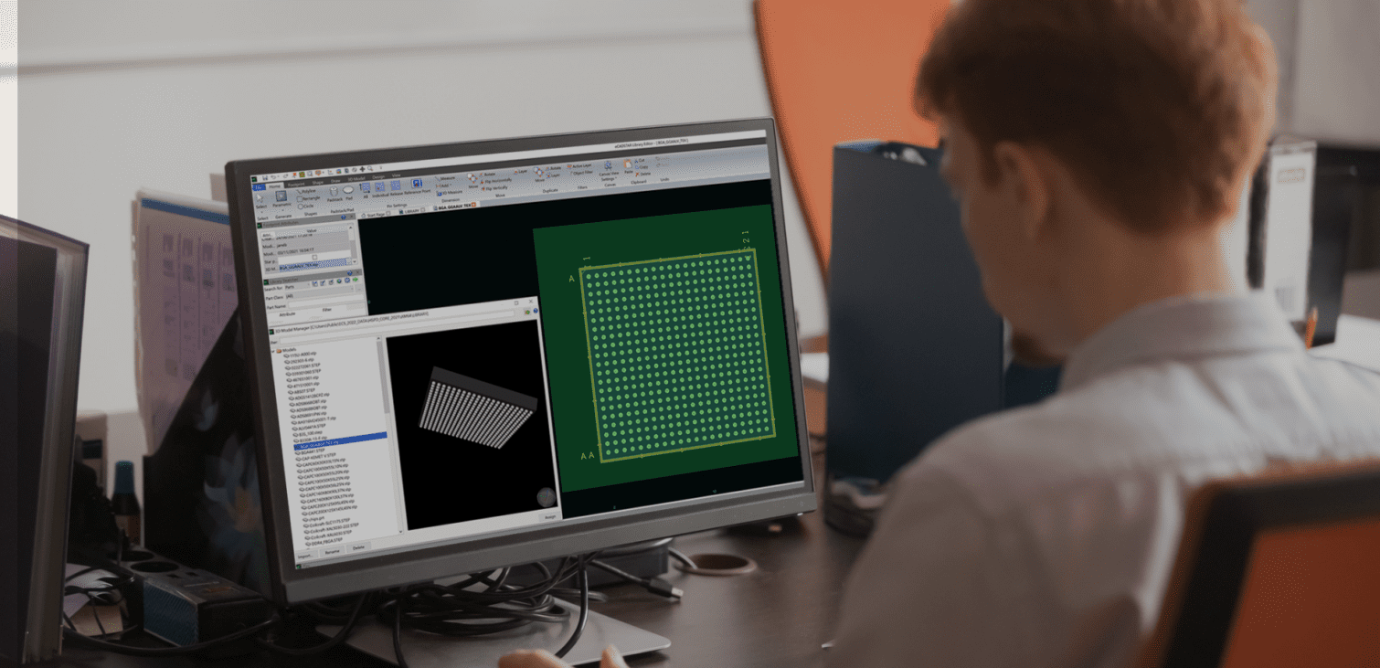
3D Model Manager
The 3D Model Manager organises your 3D models to suit your standards with fantastic 3D visibility. Rename, assign or delete 3D component models and have transparency on what each 3D model represents in your schematic and PCB library. For example, matching a corporate PCB footprint naming convention
Even organise these models into subfolders bringing structure and clarity to 3D component models, such as organising them according to package style. You can visualize these models in 3D as you manage them.
Additionally import models from a wide range of popular 3D formats, expanding your choice of 3D model sources.